

The DOI matches its Crossref record; 57 of the 60 references it cites were found in a registry or an index; none of the 10 sources its claims cite is checked for support yet.
Room-temperature waveguide-integrated photodetector using bolometric effect for mid-infrared spectroscopy applications
Open accessPublished version of a preprint
Abstract
Abstract Waveguide-integrated mid-infrared (MIR) photodetectors are pivotal components for the development of molecular spectroscopy applications, leveraging mature photonic integrated circuit (PIC) technologies. Despite various strategies, critical challenges still remain in achieving broadband photoresponse, cooling-free operation, and large-scale complementary-metal-oxide-semiconductor (CMOS)-compatible manufacturability. To leap beyond these limitations, the bolometric effect – a thermal detection mechanism – is introduced into the waveguide platform. More importantly, we pursue a free-carrier absorption (FCA) process in germanium (Ge) to create an efficient light-absorbing medium, providing a pragmatic solution for full coverage of the MIR spectrum without incorporating exotic materials into CMOS. Here, we present an uncooled waveguide-integrated photodetector based on a Ge-on-insulator (Ge-OI) PIC architecture, which exploits the bolometric effect combined with FCA. Notably, our device exhibits a broadband responsivity of 28.35%/mW across 4030–4360 nm (and potentially beyond), challenging the state of the art, while achieving a noise-equivalent power of 4.03 × 10 −7 W/Hz 0.5 at 4180 nm. We further demonstrate label-free sensing of gaseous carbon dioxide (CO 2 ) using our integrated photodetector and sensing waveguide on a single chip. This approach to room-temperature waveguide-integrated MIR photodetection, harnessing bolometry with FCA in Ge, not only facilitates the realization of fully integrated lab-on-a-chip systems with wavelength flexibility but also provides a blueprint for MIR PICs with CMOS-foundry-compatibility.
Overview
CoChat Summary
## TL;DR
The paper reports a room-temperature, waveguide-integrated mid-infrared photodetector on a Ge-on-insulator platform that uses free-carrier absorption in heavily doped Ge plus a bolometric TiO2/Ti/TiO2 stack. It achieves broadband responsivity of 28.35%/mW over 4030–4360 nm, NEP of 4.03 × 10⁻⁷ W/Hz0.5 at 4180 nm, and demonstrates on-chip label-free CO2 sensing.
## Key findings
- The device achieved a responsivity of 28.77%/mW at 4.18 μm from linear fitting at Pin > 0.3 mW, corresponding to 863.19 V/W.
- Across the measurable MIR range of 4030–4360 nm, the detector showed a broadband responsivity of about 28.35%/mW with no cutoff wavelengths.
- The noise-equivalent power was 4.03 × 10⁻⁷ W/Hz0.5 at 4.18 μm and 1 kHz, which the paper says is far better than a previously reported waveguide-integrated bolometric PD at 10.4 μW/Hz0.5 at 3.8 μm.
- In sensing, the normalized photocurrent decreased with CO2 concentration and the fitted sensitivity was 0.0696%/ppm; repeatability was shown by cycling CO2 between 100 and 250 ppm with no memory effects.
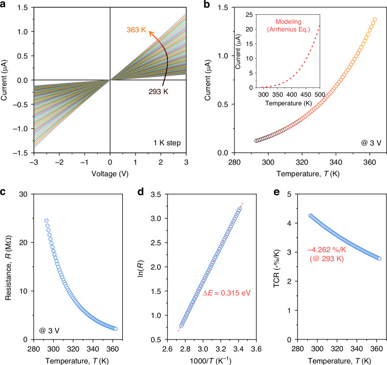
- The thermo-electrical characterization reports a TCR of −4.262%/K at 293 K and an extracted activation energy of 0.315 eV.
## Methods
- The study designed a monolithically integrated MIR PIC sensor on a Ge-OI platform with a 5-mm-long slot waveguide for sensing and a waveguide-integrated photodetector; the detector used heavily doped p+ Ge for FCA and a TiO2/Ti/TiO2 bolometric film.
- Simulations used Ansys Lumerical 3D-FDTD and HEAT solvers; fabrication involved direct wafer bonding, CMP, ion implantation (boron, 110 keV, 5 × 10^15 cm−2), annealing, and metal/dielectric deposition.
- Electrical and optical characterization included I–V and low-frequency noise measurements with a Keithley 4200A-SCS, and photoresponse/gas sensing with a QCL at 4.18–4.23 μm, lock-in detection, and calibrated optical power measurements.
## Limitations
- The paper states the device degrades beyond ~403 K due to oxidation-induced alterations in the bolometric material.
- The reported response times were constrained by the experimental setup: beam shutter open/close time for stability measurements and gas injection/removal speed for CO2 sensing.
- Evident from the text: performance and sensing demonstrations were shown under a specific setup and wavelength range, so generalization beyond the measured conditions is not directly demonstrated.
Model-written summary. Check it against the paper before relying on it.
Integrity signals
Registry
Cites
Statistics
Figures



Verification
Claims the paper makes
0 Valid · 0 Not valid · 4 Not checked · 28 Own results and interpretations
A result the paper reports from its own data — it cites no other source for it, so there is none to check. The quote shows it is in the paper.
In the paper
“there is a significant temperature rise confined within the bolometer region.”
§ Room-temperature waveguide-integrated photodetector using bolometric effect for mid-infrared spectroscopy applications > Results > Device architecture and design Figure 1a illustrates a schematic of the proposed MIR PIC-based sensor on the Ge-OI platform, comprising a slot waveguide for analyte sensing (passive sensing part) and a waveguide-integrated PD (detector part), monolithically integrated onto a single chip. Our on-chip photonic sensor utilizes light–analyte interaction within the sensing waveguide through absorption spectroscopy38,40 based on the Beer-Lambert law. An air-clad slot waveguide, supporting hollow-core guiding, has been employed to induce stronger light absorption with enhanced field confinement compared to conventional strip or rib waveguides, thus aiming to improve the sensitivity factor or to reduce the physical length of the sensing waveguide11,36,38. The residual light is then directly coupled from the sensing waveguide into the waveguide-integrated PD. As noted earlier, the operational principle of our proposed detector is the bolometric effect combined with FCA in Ge. For the bolometric material that converts light-induced temperature variations into changes in electrical resistance, we employed a TiO2/Ti/TiO2 tri-layer film, whose temperature-dependent electrical properties can be finely tailored by engineering the thickness of each layer33–35. The temperature change in bolometric detectors, in response to periodically varying incident light, can be described by231where ΔT represents the temperature change, η is the absorption efficiency for the given wavelength, ω and Φ0 are the angular frequency and the amplitude of the periodic radiation, respectively, Gth is the thermal conductance between the detector and the surrounding environment, and Cth is the thermal capacitance of the detector. As inferred from Eq. (1), increasing η, while diminishing Gth and Cth, is critical for enhancing ΔT for a given incident optical power, which directly correlates with the bolometric detector’s responsivity. In order to boost η within our PD, FCA in Ge should be elevated, which greatly depends on the type of free carriers and the doping concentration for particular wavelengths. To take full advantage of FCA in Ge, we selected heavily-doped p-type Ge (p+ Ge) as the MIR-absorbing medium (details can be found in Supplementary Note 1). For the reduction of Gth and Cth, optimizing device geometries is crucial. Here, the optimization process, including the geometrical parameters of the bolometer region – specifically, a length (LB) of 4 μm and a width (WB) of 8 μm – was conducted by considering heating efficiency, back-reflection, and in-house fabrication capabilities. The systematic process of optimizing geometries with numerical simulations is detailed in Supplementary Note 3. Figure 1b shows the simulated steady-state temperature distribution for the device designed with the final parameters. The input waveguide, having a width (Win) of 2 μm, was designed to support only the fundamental transverse-electric (TE) mode. The incoming light was set to an optical power of 1 mW at a wavelength (λ) of 4.18 μm. As depicted in Fig. 1b, there is a significant temperature rise confined within the bolometer region. This localized heat generation is achieved by FCA within the p+ Ge, which demonstrates the viability of an FCA-based thermalization process acting as a compact and efficient MIR absorber, even in the absence of resonance structures. Figure 1c, d show the optical microscope and cross-sectional transmission electron microscopy (TEM) images, respectively, of the fabricated device on the Ge-OI photonic platform featuring a 500 nm-thick top Ge, a 2 μm-thick Y2O3 BOX, and a Si substrate. Here, the proposed waveguide-integrated PD incorporates a boron-doped p+ Ge (bolometer region), a SiO2/Al2O3 (20/25 nm) insulating layer stack, a bolometric material of TiO2/Ti/TiO2 (25/2/25 nm) tri-layer film, and a Ti/W (100/150 nm) metal electrode. The thickness of each layer in the bolometric material was carefully optimized (discussed in Supplementary Fig. S7). Additional characterizations, such as X-ray photoelectron spectroscopy (XPS) and X-ray diffraction (XRD), are detailed in Supplementary Figs. S9 and S10, respectively. Energy-dispersive X-ray spectroscopy (EDS) elemental mapping (see Supplementary Fig. S11) confirms the successful deposition of each layer. Secondary-ion mass spectrometry (SIMS) depth profile analysis in Fig. 1e quantitatively reveals the impurity dopant concentration within the p+ Ge region. To make full use of FCA in Ge, ion implantation was performed with a high dopant dose of 5 × 1015 cm−2, and the implant energy was carefully adjusted to 110 keV. This optimization contributes to exposing a larger fraction of the modal field to the peak doping-concentration region of the absorbing medium, aligning with the mode-field maximum and the projected range (Rp) of the implanted ions in the p+ Ge.
plainstates a cause- Asserted: passes — The authors put it forward as true.
- Checkable: passes — It can be checked against evidence.
- Load-bearing: passes — The paper’s conclusions depend on it.
- Based: passes — The paper gives a reason why it holds.
- Rests on 2 assumptions not shown here.
A result the paper reports from its own data — it cites no other source for it, so there is none to check. The quote shows it is in the paper.
In the paper
“our device showed stable performance with a nearly flat response up to 1 kHz (the limit of our setup).”
§ Room-temperature waveguide-integrated photodetector using bolometric effect for mid-infrared spectroscopy applications > Results > Photoresponse measurement We now turn to explore the MIR photoresponse. The incident optical power coupled into the bolometer region was precisely calibrated, accounting for insertion losses from passive components with the assistance of an identical reference waveguide pattern without the detector part. A total insertion loss of 10.83 ± 0.14 dB (4.18 µm) was used for the calibration (details are provided in Supplementary Fig. S8). The un-illuminated I-V curve (off-state), plotted in the inset of Fig. 3a, reveals an off-state current (Ioff) of 127.5 nA at a 3-V bias. Figure 3a presents the change in current, calculated as the ratio of the total measured current (Iph + Ioff) to Ioff, as a function of optical power (Pin) and the corresponding responsivity (%/mW) at 4.18 μm under a 1 kHz chopping frequency, which is commonly used unit of responsivity for comparing bolometric detectors26,27,34,35. We highlight that our device achieved an R of 28.77%/mW (from linear fitting at Pin > 0.3 mW), equivalent to voltage responsivity of 863.19 V/W, which is sufficient for a wide range of MIR spectroscopy applications41–43. Details for the relationship between responsivity values in different units are described in Supplementary Note 11. This exceeds the previous state-of-the-art values for waveguide-integrated thermal-type PDs beyond 3 μm, which are 24.62%/mW at 3.8 μm in an Au antenna-assisted PD on an a-Si waveguide using the bolometric effect27, and 1.97 V/W at 3.7 μm in a graphene-based PD on a GOS waveguide using the PTE effect29. A slight nonlinearity is observed at lower Pin ranges, potentially attributed to variations in thermo-electrical properties and changes in both Gth and Cth with temperature. We also estimated the noise-equivalent power (NEP) by taking the ratio of the noise spectral density in the off-state (see Supplementary Note 7) to responsivity at 4.18 μm, calculated as 4.03 × 10⁻⁷ W/Hz0.5 at 1 kHz. Here, this far exceeds that of previously reported waveguide-integrated MIR PD using the bolometric effect (10.4 μW/Hz0.5 at 3.8 μm)27. The frequency response was analyzed by varying the chopper frequency. As illustrated in Fig. 3b, our device showed stable performance with a nearly flat response up to 1 kHz (the limit of our setup). Although higher bandwidth might be beneficial, it is not a major concern in most spectroscopy applications, unlike in telecommunications and data communications, and response times of around 1 second are common for many optical gas sensors44. This suggests that our device is sufficiently robust for MIR lab-on-a-chip systems, which can be expected to operate at a bandwidth of several tens of kHz level, based on our previous work with the Si-on-insulator (SOI) platform in the near-infrared wavelength range35. We also evaluated the spectral response in the MIR band ranging from 4030 to 4360 nm. During the measurement, the Pin was maintained within the linear fit region (Pin > 0.3 mW). As shown in Fig. 3c, our device exhibited a broadband photoresponse with an R of around 28.35%/mW across the entire measurable range without any cutoff wavelengths. Lastly, we assessed the long-term stability with switching behavior, a key parameter for evaluating PDs. Notably, as depicted in Fig. 3d, highly stable and repeatable photocurrent generation was observed without noticeable performance degradation throughout the measurements. Here, we note that the response times were constrained by the open/close time of the beam shutter. We have comprehensively compared our device’s performance with that of previously reported MIR waveguide-integrated PDs utilizing the bolometric effect, as shown in Fig. 4. Our device exhibits a broadband responsivity of ~28.35%/mW (4030–4360 nm), the highest among its counterparts. Notably, to our knowledge, no previous reports have demonstrated waveguide-integrated bolometric PDs operating beyond the wavelength range presented in this work. Traditional Si-based photonics platforms, such as SOI with a limit of ~4 μm and suspended-Si with ~8 μm, inevitably encounter wavelength limitations due to the intrinsic material absorption of SiO2 and Si in the MIR range45. Here, by leveraging the FCA-induced heating process on the Ge-OI platform that provides a broad transparency window, our approach can be widely utilized across much shorter or longer wavelength ranges in the MIR spectrum, offering significant potential for spectroscopic analysis of numerous biochemical molecules (shown in Fig. 4) without wavelength constraints. The responsivity modeling, based on FCA in Ge32 and normalized with our experimental results, is presented in Fig. 4 (red dotted line). Moreover, our device achieves a notable improvement in NEP, over 25 times greater than previously reported waveguide-integrated PDs using the bolometric effect26,27, without relying on noble metals or exotic materials, thus preserving full CMOS compatibility. Detailed performance characteristics, including comparisons with both bolometric and PTE detectors, are summarized in Supplementary Note 11.
plain- Asserted: passes — The authors put it forward as true.
- Checkable: passes — It can be checked against evidence.
- Load-bearing: unclear — It is unclear whether the paper’s conclusions depend on it.
- Based: passes — The paper gives a reason why it holds.
A result the paper reports from its own data — it cites no other source for it, so there is none to check. The quote shows it is in the paper.
In the paper
“We further demonstrate label-free sensing of gaseous carbon dioxide (CO2) using our integrated photodetector and sensing waveguide on a single chip.”
- Also stated in: § Introduction The mid-infrared (MIR) spectral region beyond 3 μm is of enormous scientific and technological importance, as it encompasses unique molecular fingerprints1–3, enabling sophisticated chemical and biological analysis in a non-invasive manner through absorption spectroscopy techniques4,5. Leveraging highly mature photonic integrated circuit (PIC) technologies6–8, substantial progress has been made in miniaturizing traditional external-optics-based spectrometers into chip-scale systems that offer cost-effective, mass-manufacturable, and scalable solutions9–12. A key bottleneck in realizing fully integrated and robust lab-on-a-chip systems is the monolithic integration of MIR photodetectors (PDs) into the waveguide platforms, which are an indispensable building block of PICs to convert light into electrical signals. Traditionally, surface-illuminated MIR PDs have relied on narrow-bandgap semiconductor materials such as HgCdTe alloy13 and III-V compounds14; yet, they necessitate cryogenic cooling (bulky and costly) to mitigate high thermal noise at room temperature, posing severe challenges in practical applications15. More recently, two-dimensional materials (e.g., graphene16 and black phosphorus17) have arisen as promising candidates that can be operated at room temperature18. However, the zero-bandgap nature of graphene results in an extremely high dark current level under biasing19. Additionally, black phosphorus itself exhibits severe performance degradation under ambient conditions and possesses an absorption edge of around 4 μm20, restricting its utility to longer wavelengths. These emerging materials also still struggle with complementary-metal-oxide-semiconductor (CMOS)-compatible processes and wafer-scale integration, impeding large-scale and cost-saving production at commercialization levels21. In this regard, it is highly beneficial for MIR photodetection to harness thermal-type PDs, where the photoresponse is extracted by converting photo-induced heat generation into the electrical signal18,22,23, enabling wavelength-insensitive photodetection by properly tailoring the spectral characteristics of the light absorber. Owing to the inherent nature of thermal detection, there is a slight compromise in response speed; however, a relatively moderate (or even low) level of bandwidth is adequate to meet the requirements for many MIR spectroscopy applications. To reap the full benefits of superior properties of the thermal detectors including wavelength independence and uncooled photodetection, here, we introduce the bolometric effect into the waveguide platform. Bolometers, a class of thermal-type PD, convert light-induced temperature fluctuations into changes in electrical resistance23–25. Notably, to date, few efforts have been devoted to achieving waveguide-integrated MIR photodetection beyond 3 μm using thermal detection mechanisms26–29. Optical absorbers with gold (Au) antennas on a suspended-Si waveguide have shown promise in bolometry in the range of 3.72–3.88 μm26,27; however, they offer low responsivities, and the resonance nature of the plasmonic structure intrinsically limits broadband photodetection. Additionally, the usage of noble metals is commonly restricted in CMOS foundries. Graphene-based detectors using the photothermoelectric (PTE) effect, another class of thermal detection mechanism based on the temperature-gradient-driven voltage generation governed by the Seebeck coefficient of the thermoelectric materials30, have shown promising results on waveguide platforms such as chalcogenide glass (ChG)-on-CaF2 at 5.2 μm28 and Ge-on-Si (GOS) at 3.7 μm29. These graphene-based PTE detectors are particularly attractive due to their zero-bias operation and fast response times. However, their usage is limited to a wavelength range of ~8 μm due to the inherent material properties of the photonic platform, which restrict their utility across the broader MIR band. In addition, the use of plasmonic Au strips29 and a split-gate architectures28,29 introduces further fabrication challenges, including misalignment and errors during transfer and patterning of graphene. A more comprehensive comparison between bolometric and PTE detectors is provided in the Discussion section. In this work, we remarkably advance the state of the art in waveguide-integrated MIR PDs by exploiting the bolometric effect with free-carrier absorption (FCA) in Ge31,32 and titanium oxide-based bolometric material33–35, providing a pragmatic approach with high fabrication robustness for uncooled MIR photodetection without foreign materials in CMOS or hybrid integrations. Our demonstration is based upon a CMOS-compatible Ge-on-insulator (Ge-OI) photonic platform with a buried oxide (BOX) of Y2O3 and a Si substrate, providing broad transparency window up to around 13 μm36–40, and reaches record-high photoresponsivity for waveguide-integrated PDs using bolometric effect beyond 3 μm. Furthermore, to demonstrate the feasibility of non-destructive, label-free detection of molecules using our room-temperature-operated waveguide-integrated MIR PD, we have experimentally conducted gaseous carbon dioxide (CO2) sensing by integrating the sensing waveguide and detector on a single chip. · boosted
“we have experimentally conducted gaseous carbon dioxide (CO2) sensing by integrating the sensing waveguide and detector on a single chip.”
§ Room-temperature waveguide-integrated photodetector using bolometric effect for mid-infrared spectroscopy applications > Abstract Waveguide-integrated mid-infrared (MIR) photodetectors are pivotal components for the development of molecular spectroscopy applications, leveraging mature photonic integrated circuit (PIC) technologies. Despite various strategies, critical challenges still remain in achieving broadband photoresponse, cooling-free operation, and large-scale complementary-metal-oxide-semiconductor (CMOS)-compatible manufacturability. To leap beyond these limitations, the bolometric effect – a thermal detection mechanism – is introduced into the waveguide platform. More importantly, we pursue a free-carrier absorption (FCA) process in germanium (Ge) to create an efficient light-absorbing medium, providing a pragmatic solution for full coverage of the MIR spectrum without incorporating exotic materials into CMOS. Here, we present an uncooled waveguide-integrated photodetector based on a Ge-on-insulator (Ge-OI) PIC architecture, which exploits the bolometric effect combined with FCA. Notably, our device exhibits a broadband responsivity of 28.35%/mW across 4030–4360 nm (and potentially beyond), challenging the state of the art, while achieving a noise-equivalent power of 4.03 × 10⁻⁷ W/Hz0.5 at 4180 nm. We further demonstrate label-free sensing of gaseous carbon dioxide (CO2) using our integrated photodetector and sensing waveguide on a single chip. This approach to room-temperature waveguide-integrated MIR photodetection, harnessing bolometry with FCA in Ge, not only facilitates the realization of fully integrated lab-on-a-chip systems with wavelength flexibility but also provides a blueprint for MIR PICs with CMOS-foundry-compatibility.
boostedstates a cause- Asserted: passes — The authors put it forward as true.
- Checkable: passes — It can be checked against evidence.
- Load-bearing: passes — The paper’s conclusions depend on it.
- Based: passes — The paper gives a reason why it holds.
- Also stated in: § Introduction The mid-infrared (MIR) spectral region beyond 3 μm is of enormous scientific and technological importance, as it encompasses unique molecular fingerprints1–3, enabling sophisticated chemical and biological analysis in a non-invasive manner through absorption spectroscopy techniques4,5. Leveraging highly mature photonic integrated circuit (PIC) technologies6–8, substantial progress has been made in miniaturizing traditional external-optics-based spectrometers into chip-scale systems that offer cost-effective, mass-manufacturable, and scalable solutions9–12. A key bottleneck in realizing fully integrated and robust lab-on-a-chip systems is the monolithic integration of MIR photodetectors (PDs) into the waveguide platforms, which are an indispensable building block of PICs to convert light into electrical signals. Traditionally, surface-illuminated MIR PDs have relied on narrow-bandgap semiconductor materials such as HgCdTe alloy13 and III-V compounds14; yet, they necessitate cryogenic cooling (bulky and costly) to mitigate high thermal noise at room temperature, posing severe challenges in practical applications15. More recently, two-dimensional materials (e.g., graphene16 and black phosphorus17) have arisen as promising candidates that can be operated at room temperature18. However, the zero-bandgap nature of graphene results in an extremely high dark current level under biasing19. Additionally, black phosphorus itself exhibits severe performance degradation under ambient conditions and possesses an absorption edge of around 4 μm20, restricting its utility to longer wavelengths. These emerging materials also still struggle with complementary-metal-oxide-semiconductor (CMOS)-compatible processes and wafer-scale integration, impeding large-scale and cost-saving production at commercialization levels21. In this regard, it is highly beneficial for MIR photodetection to harness thermal-type PDs, where the photoresponse is extracted by converting photo-induced heat generation into the electrical signal18,22,23, enabling wavelength-insensitive photodetection by properly tailoring the spectral characteristics of the light absorber. Owing to the inherent nature of thermal detection, there is a slight compromise in response speed; however, a relatively moderate (or even low) level of bandwidth is adequate to meet the requirements for many MIR spectroscopy applications. To reap the full benefits of superior properties of the thermal detectors including wavelength independence and uncooled photodetection, here, we introduce the bolometric effect into the waveguide platform. Bolometers, a class of thermal-type PD, convert light-induced temperature fluctuations into changes in electrical resistance23–25. Notably, to date, few efforts have been devoted to achieving waveguide-integrated MIR photodetection beyond 3 μm using thermal detection mechanisms26–29. Optical absorbers with gold (Au) antennas on a suspended-Si waveguide have shown promise in bolometry in the range of 3.72–3.88 μm26,27; however, they offer low responsivities, and the resonance nature of the plasmonic structure intrinsically limits broadband photodetection. Additionally, the usage of noble metals is commonly restricted in CMOS foundries. Graphene-based detectors using the photothermoelectric (PTE) effect, another class of thermal detection mechanism based on the temperature-gradient-driven voltage generation governed by the Seebeck coefficient of the thermoelectric materials30, have shown promising results on waveguide platforms such as chalcogenide glass (ChG)-on-CaF2 at 5.2 μm28 and Ge-on-Si (GOS) at 3.7 μm29. These graphene-based PTE detectors are particularly attractive due to their zero-bias operation and fast response times. However, their usage is limited to a wavelength range of ~8 μm due to the inherent material properties of the photonic platform, which restrict their utility across the broader MIR band. In addition, the use of plasmonic Au strips29 and a split-gate architectures28,29 introduces further fabrication challenges, including misalignment and errors during transfer and patterning of graphene. A more comprehensive comparison between bolometric and PTE detectors is provided in the Discussion section. In this work, we remarkably advance the state of the art in waveguide-integrated MIR PDs by exploiting the bolometric effect with free-carrier absorption (FCA) in Ge31,32 and titanium oxide-based bolometric material33–35, providing a pragmatic approach with high fabrication robustness for uncooled MIR photodetection without foreign materials in CMOS or hybrid integrations. Our demonstration is based upon a CMOS-compatible Ge-on-insulator (Ge-OI) photonic platform with a buried oxide (BOX) of Y2O3 and a Si substrate, providing broad transparency window up to around 13 μm36–40, and reaches record-high photoresponsivity for waveguide-integrated PDs using bolometric effect beyond 3 μm. Furthermore, to demonstrate the feasibility of non-destructive, label-free detection of molecules using our room-temperature-operated waveguide-integrated MIR PD, we have experimentally conducted gaseous carbon dioxide (CO2) sensing by integrating the sensing waveguide and detector on a single chip. · boosted
A result the paper reports from its own data — it cites no other source for it, so there is none to check. The quote shows it is in the paper.
In the paper
“reveals an off-state current (Ioff) of 127.5 nA at a 3-V bias.”
§ Room-temperature waveguide-integrated photodetector using bolometric effect for mid-infrared spectroscopy applications > Results > Photoresponse measurement We now turn to explore the MIR photoresponse. The incident optical power coupled into the bolometer region was precisely calibrated, accounting for insertion losses from passive components with the assistance of an identical reference waveguide pattern without the detector part. A total insertion loss of 10.83 ± 0.14 dB (4.18 µm) was used for the calibration (details are provided in Supplementary Fig. S8). The un-illuminated I-V curve (off-state), plotted in the inset of Fig. 3a, reveals an off-state current (Ioff) of 127.5 nA at a 3-V bias. Figure 3a presents the change in current, calculated as the ratio of the total measured current (Iph + Ioff) to Ioff, as a function of optical power (Pin) and the corresponding responsivity (%/mW) at 4.18 μm under a 1 kHz chopping frequency, which is commonly used unit of responsivity for comparing bolometric detectors26,27,34,35. We highlight that our device achieved an R of 28.77%/mW (from linear fitting at Pin > 0.3 mW), equivalent to voltage responsivity of 863.19 V/W, which is sufficient for a wide range of MIR spectroscopy applications41–43. Details for the relationship between responsivity values in different units are described in Supplementary Note 11. This exceeds the previous state-of-the-art values for waveguide-integrated thermal-type PDs beyond 3 μm, which are 24.62%/mW at 3.8 μm in an Au antenna-assisted PD on an a-Si waveguide using the bolometric effect27, and 1.97 V/W at 3.7 μm in a graphene-based PD on a GOS waveguide using the PTE effect29. A slight nonlinearity is observed at lower Pin ranges, potentially attributed to variations in thermo-electrical properties and changes in both Gth and Cth with temperature. We also estimated the noise-equivalent power (NEP) by taking the ratio of the noise spectral density in the off-state (see Supplementary Note 7) to responsivity at 4.18 μm, calculated as 4.03 × 10⁻⁷ W/Hz0.5 at 1 kHz. Here, this far exceeds that of previously reported waveguide-integrated MIR PD using the bolometric effect (10.4 μW/Hz0.5 at 3.8 μm)27. The frequency response was analyzed by varying the chopper frequency. As illustrated in Fig. 3b, our device showed stable performance with a nearly flat response up to 1 kHz (the limit of our setup). Although higher bandwidth might be beneficial, it is not a major concern in most spectroscopy applications, unlike in telecommunications and data communications, and response times of around 1 second are common for many optical gas sensors44. This suggests that our device is sufficiently robust for MIR lab-on-a-chip systems, which can be expected to operate at a bandwidth of several tens of kHz level, based on our previous work with the Si-on-insulator (SOI) platform in the near-infrared wavelength range35. We also evaluated the spectral response in the MIR band ranging from 4030 to 4360 nm. During the measurement, the Pin was maintained within the linear fit region (Pin > 0.3 mW). As shown in Fig. 3c, our device exhibited a broadband photoresponse with an R of around 28.35%/mW across the entire measurable range without any cutoff wavelengths. Lastly, we assessed the long-term stability with switching behavior, a key parameter for evaluating PDs. Notably, as depicted in Fig. 3d, highly stable and repeatable photocurrent generation was observed without noticeable performance degradation throughout the measurements. Here, we note that the response times were constrained by the open/close time of the beam shutter. We have comprehensively compared our device’s performance with that of previously reported MIR waveguide-integrated PDs utilizing the bolometric effect, as shown in Fig. 4. Our device exhibits a broadband responsivity of ~28.35%/mW (4030–4360 nm), the highest among its counterparts. Notably, to our knowledge, no previous reports have demonstrated waveguide-integrated bolometric PDs operating beyond the wavelength range presented in this work. Traditional Si-based photonics platforms, such as SOI with a limit of ~4 μm and suspended-Si with ~8 μm, inevitably encounter wavelength limitations due to the intrinsic material absorption of SiO2 and Si in the MIR range45. Here, by leveraging the FCA-induced heating process on the Ge-OI platform that provides a broad transparency window, our approach can be widely utilized across much shorter or longer wavelength ranges in the MIR spectrum, offering significant potential for spectroscopic analysis of numerous biochemical molecules (shown in Fig. 4) without wavelength constraints. The responsivity modeling, based on FCA in Ge32 and normalized with our experimental results, is presented in Fig. 4 (red dotted line). Moreover, our device achieves a notable improvement in NEP, over 25 times greater than previously reported waveguide-integrated PDs using the bolometric effect26,27, without relying on noble metals or exotic materials, thus preserving full CMOS compatibility. Detailed performance characteristics, including comparisons with both bolometric and PTE detectors, are summarized in Supplementary Note 11.
plain- Asserted: passes — The authors put it forward as true.
- Checkable: passes — It can be checked against evidence.
- Load-bearing: unclear — It is unclear whether the paper’s conclusions depend on it.
- Based: passes — The paper gives a reason why it holds.
A result the paper reports from its own data — it cites no other source for it, so there is none to check. The quote shows it is in the paper.
In the paper
“A nearly-linear characteristics with Ohmic behavior between the bolometric material and the electrode stack was obviously observed.”
§ Room-temperature waveguide-integrated photodetector using bolometric effect for mid-infrared spectroscopy applications > Results > Thermo-electrical characterization We first investigated the temperature-dependent electrical properties. Figure 2a shows the current-voltage (I-V) curves from a voltage sweep ranging from −3.0 V to +3.0 V, with a 0.01-V interval, measured from 293 K to 363 K (1-K step), limited by our Peltier-driven stage. A nearly-linear characteristics with Ohmic behavior between the bolometric material and the electrode stack was obviously observed. Figure 2b plots the temperature-dependent current values at 3-V derived from the I-V curves, demonstrating a significant relationship with the temperature. Figure 2c presents the resistance-temperature (R-T) characteristics under constant-voltage mode, which can be modeled following equation to estimate the activation energy (ΔE):2where R(T) denotes the temperature-dependent electrical resistance, T is the absolute temperature, Ro is a constant, and kB is the Boltzmann constant. From Eq. (2), ΔE is extracted from the slope of the Arrhenius plot (ln(R) vs. 1000/T) shown in Fig. 2d, which was determined to be 0.315 eV within the measured temperature range. The temperature-dependent current modeling over a high-temperature range, based on the Arrhenius relationship by Eq. (2), is described in the inset of Fig. 2b, revealing a rapid, exponential increase in electrical current with rising temperature. However, beyond the certain threshold temperature range (~403 K), our device undergoes degradation due to oxidation-induced alterations in the structural properties of the bolometric material (as detailed in Supplementary Note 6). To quantify the temperature dependence of the electrical resistance, temperature-coefficient of resistance (TCR), a crucial performance indicator for bolometric detectors, is introduced, which is defined as the derivative of resistance with respect to temperature,3
boostedstates an association- Asserted: passes — The authors put it forward as true.
- Checkable: passes — It can be checked against evidence.
- Load-bearing: unclear — It is unclear whether the paper’s conclusions depend on it.
- Based: passes — The paper gives a reason why it holds.
17 more claims
Create a free account to see all 32 claims and to verify the 1 reference still open.
- It may state two separate claims as one. 5
- Probably not a substantial claim. 5
Citations
Cites
Graphene photonics and optoelectronics
Bonaccorso, F., Sun, Z., Hasan, T., & Ferrari, A. C. (2010) · Nature Photonics · doi:10.1038/nphoton.2010.186 · Cited by 7,726 · cited 1×
“However, the zero-bandgap nature of graphene results in an extremely high dark current level under biasing 19 .”
The HITRAN2020 molecular spectroscopic database
Gordon, I. E., Rothman, L. S., Hargreaves, R. J., Hashemi, R., Karlovets, E. V., Skinner, F. M., Conway, E. K., Hill, C., Kochanov, R. V., Tan, Y., et al. (2022) · Journal of Quantitative Spectroscopy and Radiative Transfer · doi:10.1016/j.jqsrt.2021.107949 · Cited by 2,600
Hodgkinson, J., & Tatam, R. P. (2013) · Measurement Science and Technology · doi:10.1088/0957-0233/24/1/012004 · Cited by 1,745 · cited 1×
“Although higher band-width might be bene fi cial, it is not a major concern in most spectroscopy applications, unlike in tele-communications and data communications, and response times of around 1 second are common for many optical gas sensors 44 .”
Mid-infrared plasmonic biosensing with graphene
Rodrigo, D., Limaj, O., Janner, D., Etezadi, D., García de Abajo, F. J., Pruneri, V., & Altug, H. (2015) · Science · doi:10.1126/science.aab2051 · Cited by 1,462 · cited 12×
“Details for the relationship between responsivity values in different units are described in Supplementary Note 11.”
InfluentialSingle-chip microprocessor that communicates directly using light
Sun, C., Wade, M. T., Lee, Y., Orcutt, J. S., Alloatti, L., Georgas, M. S., Waterman, A. S., Shainline, J. M., Avizienis, R. R., Lin, S., et al. (2015) · Nature · doi:10.1038/nature16454 · Cited by 1,308 · cited 12×
“Details for the relationship between responsivity values in different units are described in Supplementary Note 11.”
InfluentialEnvironmental instability of few-layer black phosphorus
Island, J. O., Steele, G. A., Zant, H. S. J. V. D., & Castellanos-Gomez, A. (2015) · 2D Materials · doi:10.1088/2053-1583/2/1/011002 · Cited by 954 · cited 1×
“Additionally, black phosphorus itself exhibits severe performance degradation under ambient conditions and possesses an absorption edge of around 4 μ m 20 , restricting its utility to longer wavelengths.”
Integrating photonics with silicon nanoelectronics for the next generation of systems on a chip
Atabaki, A. H., Moazeni, S., Pavanello, F., Gevorgyan, H., Notaros, J., Alloatti, L., Wade, M. T., Sun, C., Kruger, S. A., Meng, H., et al. (2018) · Nature · doi:10.1038/s41586-018-0028-z · Cited by 927 · cited 11×
“Details for the relationship between responsivity values in different units are described in Supplementary Note 11.”
InfluentialCompact spectrometer based on a disordered photonic chip
Redding, B., Liew, S. F., Sarma, R., & Cao, H. (2013) · Nature Photonics · doi:10.1038/nphoton.2013.190 · Cited by 667 · cited 1×
“Furthermore, employing computational spectroscopy techniques, particularly through disordered structures 9,56,57 , could serve as a strategy to minimize system footprint and power consumption while improving robust and agile multiplexed-detection capabilities.”
Silicon/2D-material photodetectors: from near-infrared to mid-infrared
Liu, C., Guo, J., Yu, L., Li, J., Zhang, M., Li, H., Shi, Y., & Dai, D. (2021) · Light: Science & Applications · doi:10.1038/s41377-021-00551-4 · Cited by 473 · cited 2×
“More recently, two-dimensional materials (e.g., graphene 16 and black phosphorus 17 ) have arisen as promising candidates that can be operated at room temperature 18 .”
Ultra-fast germanium photodiode with 3-dB bandwidth of 265 GHz
Lischke, S., Peczek, A., Morgan, J. S., Sun, K., Steckler, D., Yamamoto, Y., Korndörfer, F., Mai, C., Marschmeyer, S., Fraschke, M., et al. (2021) · Nature Photonics · doi:10.1038/s41566-021-00893-w · Cited by 349 · cited 1×
“…we can potentially push the photoresponse to a much higher level through various strategies, such as scaling down the width of bolometer region and implementing a top-contact electrode scheme above the dielectric cladding with via plugs 52 , improving heat con-fi nement within the absorbing medium.”
Cited by
2D material-based infrared photodetectors: recent progress, challenges, and perspectives
Zulfiqar, M. W., Nisar, S., Dastgeer, G., Rabeel, M., Ghazanfar, H., Ali, A., Imran, M., Kim, H., & Kim, D. (2025) · Nanoscale · doi:10.1039/d5nr01920f · Cited by 42
Jiang, M., Zhao, Y., Liu, T., et al. (2025) · Light Science & Applications · doi:10.1038/s41377-025-01991-y · Cited by 22
“S5 and Supplementary Note 3.”
InfluentialLin, H., Zheng, H., Zhu, W., Zhong, Y., Yu, J., Wu, H., Jia, Z., Zhang, J., Sampaolo, A., Patimisco, P., et al. (2026) · Nature Communications · doi:10.1038/s41467-026-69042-7 · Cited by 28
“Breakthroughs in LN photonics have propelled the development in high-performance components, including electro-optic modulators 3 – 5 , frequency shifters 6 , frequency combs 7 – 9 , pulse generators 10 , tunable lasers 11 , spectroscopic sensing 12 – 14 and photonic integrated circuits 15 .”
Mid‐Infrared Integrated Photonics: Material Platforms and Emerging Applications
Butt, M. A., Abellán, D. P., & Piramidowicz, R. (2025) · Laser & Photonics Review · doi:10.1002/lpor.202500099 · Cited by 29
“In healthcare, MIR techniques are used for non-invasivediagnostics,suchasdetectingglucoselevelsorearly-stage cancer biomarkers by analyzing breath or skin samples [11, 12].”
Yan, T., Li, L., Hao, J., et al. (2025) · ACS Photonics · doi:10.1021/acsphotonics.5c01684 · Cited by 6
Metadata
- Authors
- Shim, J., Lim, J., Kim, I., Jeong, J., Kim, B. H., Kim, S. K., Geum, D.-M., & Kim, S.
- Affiliations
- Korea Advanced Institute of Science and Technology (KR)
- Inha University (KR)
- Corresponding author
- Kim, SangHyeon
- Venue
- Light: Science & Applications
- Published
- 2025-03-19
- Volume
- 14
- Issue
- 1
- Pages
- 125-125
- ISSN
- 2047-7538 (ISSN-L)
- PMC
- PMC11920593
- OpenAlex
- W4408553954
- Cited by
- 31
- References
- 60
- Citations by year
- 2026: 19 · 2025: 12
- FWCI
- 6.89
- Type
- journal article
- Language
- en
- Open access
- gold
- doi.org
- Licence
- cc-by
- creativecommons.org/licenses/by/4.0 (tdm)
- creativecommons.org/licenses/by/4.0 (vor)
- Locations
- Light Science & Applications (publishedVersion, cc-by)
- Research Square (acceptedVersion, cc-by)
- PubMed Central (publishedVersion, cc-by)
- PubMed (publishedVersion)
- arXiv (Cornell University) (submittedVersion)
- DOAJ (DOAJ: Directory of Open Access Journals) (submittedVersion, cc-by-sa)
- Figshare (submittedVersion, cc-by)
- arXiv (Cornell University)
- Funders
- National Research Foundation of Korea (2023R1A2C2002777, 2020M3H4A3081735)
- Korea Institute of Science and Technology (2E33052)
- BK21 FOUR
- Topics
- Physical Sciences › Engineering › Electrical and Electronic Engineering › Photonic and Optical Devices
- Physical Sciences › Chemistry › Spectroscopy › Spectroscopy and Laser Applications
- Physical Sciences › Engineering › Electrical and Electronic Engineering › Advanced Semiconductor Detectors and Materials
- Keywords
- mid-infrared photodetectors, waveguide-integrated photodetectors, bolometric effect, free carrier absorption, germanium-on-insulator, noise equivalent power, carbon dioxide detection, lab-on-a-chip, mid-infrared spectroscopy
About these checks
Registry, retraction, Cites and statistics results are computed, not judged, with one exception: a printed reference that no index lists is read once by a model before it counts as a citation error. Claims are extracted by a model and kept only when their quote appears verbatim in the text; each cited source is then checked, with a model’s help, for whether it says what the claim relies on. Those verdicts can be wrong — read the claim’s quote and the cited source before relying on one.
A language model drew the claims from the paper on 2026-10-10, under version 3 of the claim definition (model deepseek-v4.1-flash, prompt extract-v3).
A second model labelled each claim on 2026-10-10 (model jev-1.13-20260917, definition revision gold-guideline-v0.2).
Statistics and arithmetic are recomputed, not judged.
Confidence bands are shown only for fields calibrated on our annotated test set. None is calibrated yet, so no band is shown.
What counts as a claim ›How we measure confidence ›How we check this ›
Are you an author, or do you see a problem with this page? Request a review
How to cite
Cite CoChat for the checks on this page, and the paper for its own findings.
- This page
- CoChat. (2026). Citation check: Room-temperature waveguide-integrated photodetector using bolometric effect for mid-infrared spectroscopy applications. https://app.cochat.ai/papers/10.1038/s41377-025-01803-3
- The paper
- Shim, J., Lim, J., Kim, I., Jeong, J., Kim, B. H., Kim, S. K., Geum, D.-M., & Kim, S. (2025). Room-temperature waveguide-integrated photodetector using bolometric effect for mid-infrared spectroscopy applications. Light: Science & Applications. https://doi.org/10.1038/s41377-025-01803-3
Data sources
Bibliographic data: Semantic Scholar, OpenAlex, Crossref.
Contains information from the Semantic Scholar Academic Graph Datasets, made available under the ODC Attribution License (ODC-BY 1.0).
Semantic Scholar’s data is described in: Kinney, R., et al. (2023). The Semantic Scholar Open Data Platform. arXiv:2301.10140.
