

The DOI matches its Crossref record; 11 of the 11 references it cites were found in a registry or an index.
Experimental Realization of a Reflections-Free Compact Delay Line Based on a Photonic Topological Insulator
Abstract
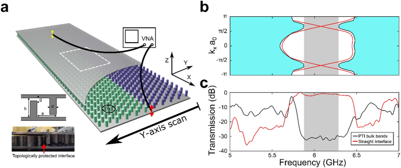
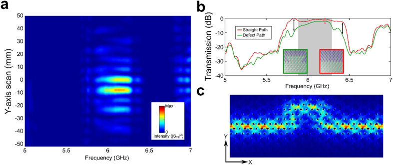
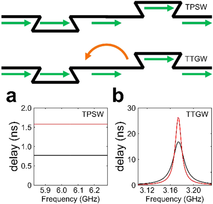
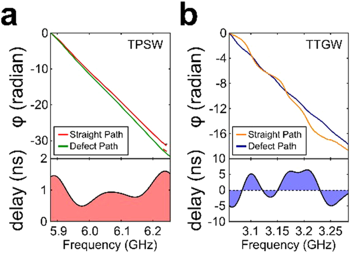
Electromagnetic (EM) waves propagating through an inhomogeneous medium are generally scattered whenever the medium’s electromagnetic properties change on the scale of a single wavelength. This fundamental phenomenon constrains how optical structures are designed and interfaced with each other. Recent theoretical work indicates that electromagnetic structures collectively known as photonic topological insulators (PTIs) can be employed to overcome this fundamental limitation, thereby paving the way for ultra-compact photonic structures that no longer have to be wavelength-scale smooth. Here we present the first experimental demonstration of a photonic delay line based on topologically protected surface electromagnetic waves (TPSWs) between two PTIs which are the EM counterparts of the quantum spin-Hall topological insulators in condensed matter. Unlike conventional guided EM waves that do not benefit from topological protection, TPSWs are shown to experience multi-wavelength reflection-free time delays when detoured around sharply-curved paths, thus offering a unique paradigm for compact and efficient wave buffers and other devices.
Overview
The claims and statistics of this paper haven’t been checked yet.
Run the check — free, no account needed. It reads the open-access text and checks the sources it cites.
Integrity signals
Registry
Cites
Statistics
Figures
Verification
Claims the paper makes
The claims and statistics of this paper haven’t been checked yet.
Run the check — free, no account needed. It reads the open-access text and checks the sources it cites.
Claims other papers make about this one
Each is checked against this paper’s own text: does it say what the citing paper says it does?
The cited source says what the claim attributes to it.
In the citing paper
“The following works have shown that topological photonic states displaying the photonic analog of the quantum spin Hall effect can also be realized in an even more simple structure, as recently proposed (Ma et al., 2015) and experimentally realized (Cheng et al., 2016;Lai et al., 2016;Xiao et al., 2016).”
From Topological photonics (2019) · cites this paper as Lai et al., 2016
Self-check
Percentages, sums and reported differences re-computed from the paper’s own numbers.
The self-check needs the paper’s full text.
Citations
Cites
Quantum Spin Hall Insulator State in HgTe Quantum Wells
König, M., Wiedmann, S., Brüne, C., Roth, A., Buhmann, H., Molenkamp, L. W., Qi, X.-L., & Zhang, S.-C. (2007) · Science · doi:10.1126/science.1148047 · Cited by 6,151
A topological Dirac insulator in a quantum spin Hall phase
Hsieh, D., Qian, D., Wray, L., Xia, Y., Hor, Y. S., Cava, R. J., & Hasan, M. Z. (2008) · Nature · doi:10.1038/nature06843 · Cited by 3,523
Photonic Floquet topological insulators
Rechtsman, M. C., Zeuner, J. M., Plotnik, Y., Lumer, Y., Podolsky, D., Dreisow, F., Nolte, S., Segev, M., & Szameit, A. (2013) · Nature · doi:10.1038/nature12066 · Cited by 3,332
Observation of unidirectional backscattering-immune topological electromagnetic states
Wang, Z., Chong, Y., Joannopoulos, J. D., & Soljačić, M. (2009) · Nature · doi:10.1038/nature08293 · Cited by 3,123
Bogaerts, W., De Heyn, P., Van Vaerenbergh, T., De Vos, K., Kumar Selvaraja, S., Claes, T., Dumon, P., Bienstman, P., Van Thourhout, D., & Baets, R. (2012) · Laser & Photonics Reviews · doi:10.1002/lpor.201100017 · Cited by 2,643
Reflection-Free One-Way Edge Modes in a Gyromagnetic Photonic Crystal
Wang, Z., Chong, Y. D., Joannopoulos, J. D., & Soljačić, M. (2008) · Physical Review Letters · doi:10.1103/physrevlett.100.013905 · Cited by 1,444
Experimental realization of photonic topological insulator in a uniaxial metacrystal waveguide
Chen, W.-J., Jiang, S.-J., Chen, X.-D., Zhu, B., Zhou, L., Dong, J.-W., & Chan, C. T. (2014) · Nature Communications · doi:10.1038/ncomms6782 · Cited by 555
Ma, T., Khanikaev, A. B., Mousavi, S. H., & Shvets, G. (2015) · Physical Review Letters · doi:10.1103/physrevlett.114.127401 · Cited by 393
Self-citationArtificial gauge field for photons in coupled cavity arrays
Umucalılar, R. O., & Carusotto, I. (2011) · Physical Review A · doi:10.1103/physreva.84.043804 · Cited by 300
PT-symmetry in honeycomb photonic lattices
Szameit, A., Rechtsman, M. C., Bahat-Treidel, O., & Segev, M. (2011) · Physical Review A · doi:10.1103/physreva.84.021806 · Cited by 280
Research works printed but not linked: 24
- Haldane, F. & Raghu, S. Possible realization of directional optical waveguides in photonic crystals with broken time-reversal symmetry. Phys. Rev. Lett. 100, 013904 (2008). · DOI · Paper page
- Poo, Y., Wu, R., Lin, Z., Yang, Y. & Chan, C. T. Experimental Realization of Self-Guiding Unidirectional Electromagnetic Edge States. Phys. Rev. Lett. 106, 093903 (2011). · DOI
- Raghu, S. & Haldane, F. Analogs of quantum-Hall-effect edge states in photonic crystals. Physical Review A 78(3), 033834 (2008). · DOI · Paper page
- Hafezi, M., Demler, E. A., Lukin, M. D. & Taylor, J. M. Robust optical delay lines with topological protection. Nature Physics 7(11), 907–912 (2011). · DOI · Paper page
- Hafezi, M., Mittal, S., Fan, J., Migdall, A. & Taylor, J. M. Imaging topological edge states in silicon photonics. Nature Photonics 7, 1001–1005 (2013). · DOI · Paper page
- Fang, K., Yu, Z. & Fan, S. Realizing effective magnetic field for photons by controlling the phase of dynamic modulation. Nature Photonics 6(11), 782–787 (2012). · DOI · Paper page
- Khanikaev, A. B. et al. Photonic topological insulators. Nature Materials 12(3), 233–239 (2013). · DOI · Paper page
- Lu, L., Joannopoulos, J. & Soljačić, M., Topological photonics. Nature Photonics 8, 821 (2014). · DOI · Paper page
- Wang, Z. & Fan, S. Optical circulators in two-dimensional magneto-optical photonic crystals. Opt. Lett. 30, 1989 (2005). · DOI · Paper page
- Qiu, W., Wang, Z. & Soljačić, M. Broadband circulators based on directional coupling of one-way waveguides. Opt. Express 19, 22248 (2011). · DOI
- Wallace, J. W. & Jensen, M. A., Mutual Coupling in MIMO Wireless Systems: A Rigorous Network Theory Analysis. IEEE Transactions on Wireless Communications 3, 1317 (2004). · DOI
- Xia, F., Sekaric, L. & Vlasov, Y. Ultacompact optical buffers on a silicon chip. Nature Photonics 1, 65 (2007). · DOI
- Mittal, S. et al. Topologically Robust Transport of Photons in a Synthetic Gauge Field. Phys. Rev. Lett. 113, 087403 (2014). · DOI
- Kane, C. L. & Mele, E. J. Quantum Spin Hall Effect in Graphene. Phys. Rev. Lett. 95, 226801 (2005). · DOI · Paper page
- Bernevig, B. A. & Zhang, S.-C. Quantum Spin Hall Effect. Phys. Rev. Lett. 96, 106802 (2006). · DOI · Paper page
- Chabanov, A. & Genack, A. Statistics of Dynamics of Localized Waves. Phys. Rev. Lett. 87, 233903 (2001). · DOI · Paper page
- Karl, N. J., McKinney, R. W., Monnai, Y., Mendis, R. & Mittleman, D. M. Frequency-division multiplexing in the terahertz range using a leaky-wave antenna. Nature Photonics 9, 717 (2015). · DOI
- Sheng, D. N., Weng, Z. Y., Sheng, L. & Haldane, F. D. M. Quantum Spin-Hall Effect and Topologically Invariant Chern Numbers. Phys. Rev. Lett. 97(3), 036808 (2006). · DOI · Paper page
- Rainwater, D. et al. Experimental verification of three-dimensional plasmonic cloaking in free-space. New J. Physics 14, 013054 (2012). · DOI
- Xu, S. et al. Broadband surface-wave transformation cloak. PNAS 112, 7635 (2015). · DOI
- Fan, S., Villeneuve, P. R., Joannopoulos, J. D. & Haus, H. Channel drop tunneling through localized states. Physical Review Letters 80(5), 960 (1998). · DOI
- Meade, R. D., Brommer, K. D., Rappe, A. M. & Joannopoulos, J. Electromagnetic Bloch waves at the surface of a photonic crystal. Physical Review B 44(19), 10961 (1991). · DOI
- Sebbah, P., Legrand, O. & Genack, A. Fluctuations in photon local delay time and their relation to phase spectra in random media. Phys. Rev. E 59, 2406 (1999). · DOI
- Bhattacharjee, S. et al. Folded Waveguide Traveling Wave Tube Sources For Terahertz Radiation. IEEE Transactions on Plasma Science 32, 1002 (2004). · DOI
Cited by
Sorted by citations
Ozawa, T., Price, H. M., Amo, A., Goldman, N., Hafezi, M., Lu, L., Rechtsman, M. C., Schuster, D., Simon, J., Zilberberg, O., et al. (2019) · Reviews of Modern Physics · doi:10.1103/revmodphys.91.015006 · Cited by 3,722
Photonic quantum information processing: a review
Flamini, F., Spagnolo, N., & Sciarrino, F. (2019) · Reports on Progress in Physics · doi:10.1088/1361-6633/aad5b2 · Cited by 770
Scattering-free edge states between heterogeneous photonic topological insulators
Ma, T., & Shvets, G. (2017) · Physical Review B · doi:10.1103/physrevb.95.165102 · Cited by 122
Self-citation
Metadata
- Authors
- Lai, K., Ma, T., Bo, X., Anlage, S., & Shvets, G.
- Venue
- Scientific Reports
- Published
- 2016-06-27
- Volume
- 6
- Issue
- 1
- ISSN
- 2045-2322
- PMC
- PMC4921924
- Cited by
- 70
- References
- 11
- Language
- en
About these checks
Registry, retraction, Cites and statistics results are computed, not judged, with one exception: a printed reference that no index lists is read once by a model before it counts as a citation error. Claims are extracted by a model and kept only when their quote appears verbatim in the text; each cited source is then checked, with a model’s help, for whether it says what the claim relies on. Those verdicts can be wrong — read the claim’s quote and the cited source before relying on one.
Statistics and arithmetic are recomputed, not judged.
Confidence bands are shown only for fields calibrated on our annotated test set. None is calibrated yet, so no band is shown.
What counts as a claim ›How we measure confidence ›How we check this ›
Are you an author, or do you see a problem with this page? Request a review
