

The DOI matches its Crossref record.
Translational MEMS Platform for Planar Optical Switching Fabrics
Open accessAbstract
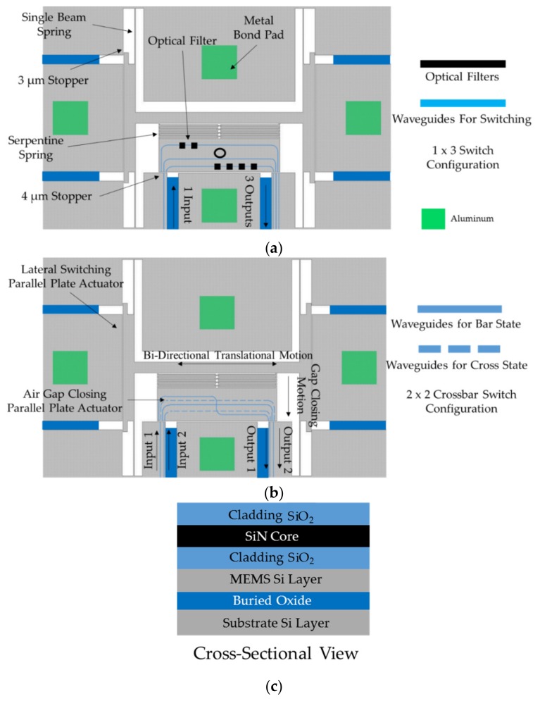
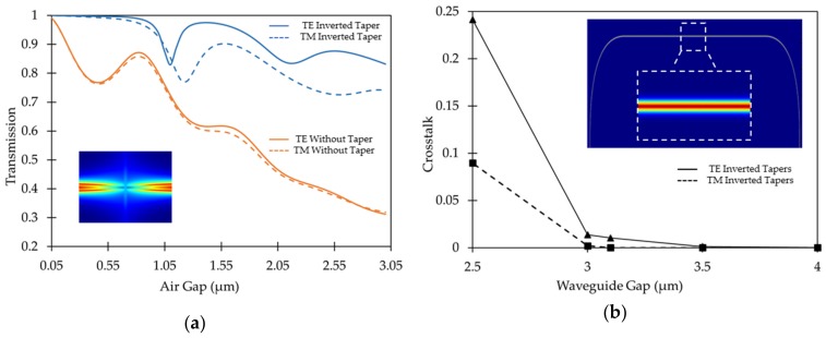
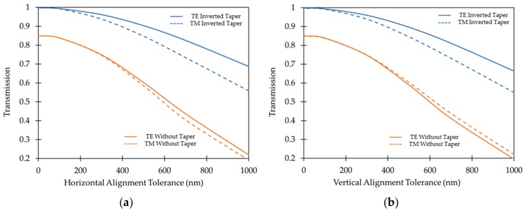
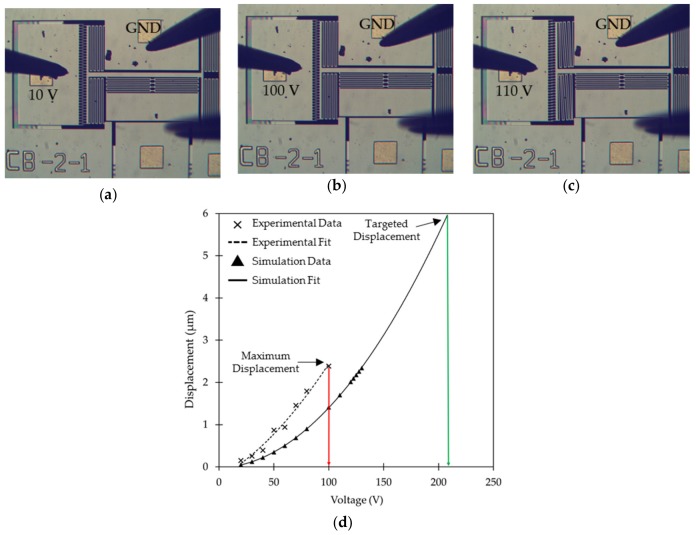
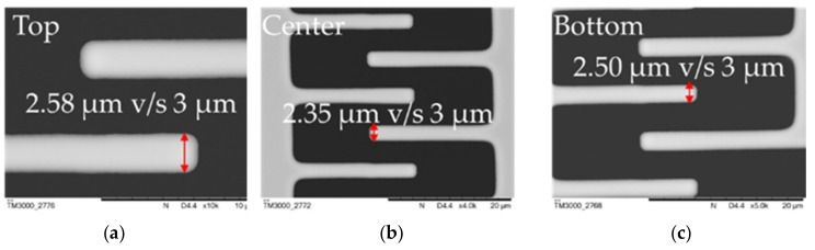
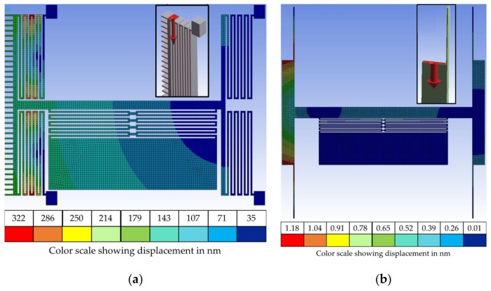
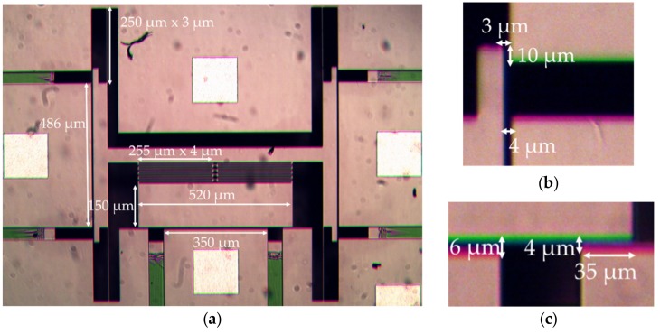
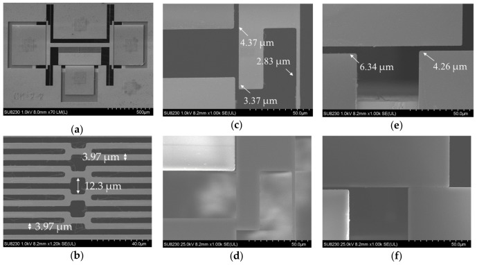
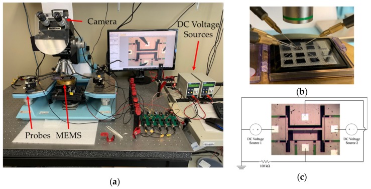
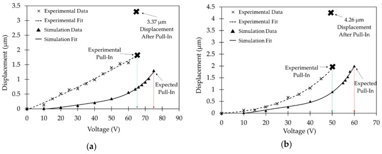
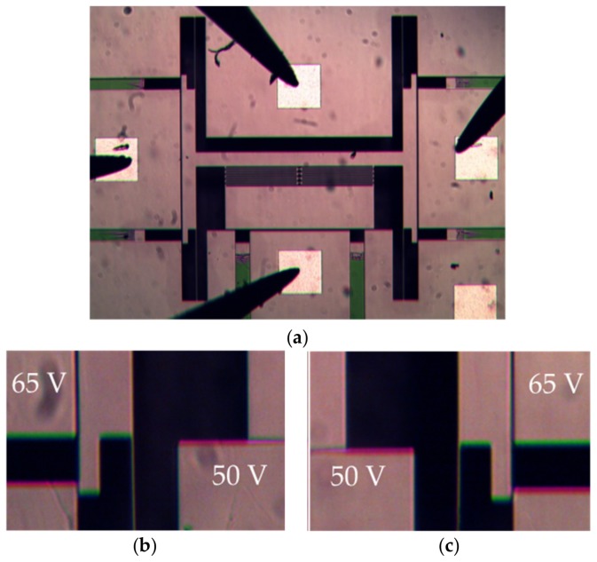
While 3-D microelectromechanical systems (MEMS) allow switching between a large number of ports in optical telecommunication networks, the development of such systems often suffers from design, fabrication and packaging constraints due to the complex structures, the wafer bonding processes involved, and the tight alignment tolerances between different components. In this work, we present a 2-D translational MEMS platform capable of highly efficient planar optical switching through integration with silicon nitride (SiN) based optical waveguides. The discrete lateral displacement provided by simple parallel plate actuators on opposite sides of the central platform enables switching between different input and output waveguides. The proposed structure can displace the central platform by 3.37 µm in two directions at an actuation voltage of 65 V. Additionally, the parallel plate actuator designed for closing completely the 4.26 µm air gap between the fixed and moving waveguides operates at just 50 V. Eigenmode expansion analysis shows over 99% butt-coupling efficiency the between the SiN waveguides when the gap is closed. Also, 2.5 finite-difference time-domain analysis demonstrates zero cross talk between two parallel SiN waveguides across the length of the platform for a 3.5 µm separation between adjacent waveguides enabling multiple waveguide configuration onto the platform. Different MEMS designs were simulated using static structural analysis in ANSYS. These designs were fabricated with a custom process by AEPONYX Inc. (Montreal, QC, Canada) and through the PiezoMUMPs process of MEMSCAP (Durham, NC, USA).
Overview
The claims and statistics of this paper haven’t been checked yet.
Run the check — free, no account needed. It reads the open-access text and checks the sources it cites.
Integrity signals
Registry
Cites
Statistics
Figures
Verification
Claims the paper makes
The claims and statistics of this paper haven’t been checked yet.
Run the check — free, no account needed. It reads the open-access text and checks the sources it cites.
Claims other papers make about this one
Each is checked against this paper’s own text: does it say what the citing paper says it does?
The source backs part of the claim, not all of it — or backs it for a different population, condition or comparison.
In the citing paper
“Optical simulation results for vertical misalignment between the suspended and fixed waveguides performed in our previous work also show that a 10 nm to 18 nm misalignment has negligible effect on the optical performance of the switch [29].”
From Integrated 1 × 3 MEMS silicon nitride photonics switch (2022) · cites this paper as [29]
Experimental — accuracy not yet measuredThe cited source says what the claim attributes to it.
In the citing paper
“During our experiments we also found that some of the devices shorted during switching unlike our previous work, which involved testing only the MEMS actuators for translational motion [29].”
From Integrated 1 × 3 MEMS silicon nitride photonics switch (2022) · cites this paper as [29]
The cited source says what the claim attributes to it.
In the citing paper
“This is significantly higher than the 65 V pull-in voltage for the switching actuator with a 10 µm device layer [29].”
From Integrated 1 × 3 MEMS silicon nitride photonics switch (2022) · cites this paper as [29]
The cited source says what the claim attributes to it.
In the citing paper
“Also, the use of springs made of a single beam anchored at opposite ends provided enough planar vertical stiffness to avoid rotation of the platform during its displacement.”
From Integrated 1 × 3 MEMS silicon nitride photonics switch (2022) · cites this paper as [29]
The cited source says what the claim attributes to it.
In the citing paper
“The gap closing actuator showed electrostatic pull-in at 62 V with a 59 µm device layer in comparison to 50 V for a 10 µm device layer [29].”
From Integrated 1 × 3 MEMS silicon nitride photonics switch (2022) · cites this paper as [29]
The cited source says what the claim attributes to it.
In the citing paper
“In our previous work [29], translational MEMS actuators with a single beam spring required a switching voltage of 65 V.”
From Integrated 1 × 3 MEMS silicon nitride photonics switch (2022) · cites this paper as [29]
Self-check
Percentages, sums and reported differences re-computed from the paper’s own numbers.
The self-check needs the paper’s full text.
Citations
Cites
Still being checked.
Research works printed but not linked: 47
- Monk, 1995, The Digital Micromirror Device for Projection Display Deformable Membrane Displays, Microelectron. Eng., 27, 489, 10.1016/0167-9317(94)00151-J · DOI
- Baran, 2014, MEMS laser scanners: A review, J. Microelectromech. Syst., 23, 259, 10.1109/JMEMS.2013.2295470 · DOI
- Hammadi, 2014, A survey on architectures and energy efficiency in Data Center Networks, Comput. Commun., 40, 1, 10.1016/j.comcom.2013.11.005 · DOI
- Farrington, 2010, Helios: A Hybrid Electrical/Optical Switch Architecture for Modular Data Centers, ACM SIGCOMM Comput. Commun. Rev., 40, 339, 10.1145/1851275.1851223 · DOI
- Prescott, 2015, Scaled Out Optically Switched (SOOS) network architecture for Web Scale Data Centers, 2015 IEEE Opt. Interconnects Conf. (OI), 15, 90
- Kim, 2003, 1100 × 1100 Port MEMS-Based Optical Crossconnect With 4-dB Maximum Loss, IEEE Photonics Technol. Lett., 15, 1537, 10.1109/LPT.2003.818653 · DOI
- Fernandez, 2004, Modular MEMS design and fabrication for an 80 × 80 transparent optical cross-connect switch, Proc. SPIE, 5604, 208, 10.1117/12.581901 · DOI
- Aksyuk, 2003, Lucent Microstar micromirror array technology for large optical crossconnects, MOEMS Miniaturized Syst., 4178, 320, 10.1117/12.396503 · DOI
- Li, 2011, Design, fabrication and characterization of a high fill-factor micromirror array for wavelength selective switch applications, Sens. Actuators A Phys., 171, 274, 10.1016/j.sna.2011.07.001 · DOI
- Liu, 2013, Large size MEMS scanning mirror with vertical comb drive for tunable optical filter, Opt. Lasers Eng., 51, 54, 10.1016/j.optlaseng.2012.07.019 · DOI
- Koh, 2010, A piezoelectric-driven three-dimensional MEMS VOA using attenuation mechanism with combination of rotational and translational effects, J. Microelectromech. Syst., 19, 1370, 10.1109/JMEMS.2010.2076785 · DOI
- Microactuator, 2012, Improved Designs for an Electrothermal In-Plane Microactuator, J. Microelectromech. Syst., 21, 586, 10.1109/JMEMS.2012.2185820 · DOI
- Member, 2003, MOEMS Tuning Element for a Littrow External Cavity Laser, J. Microelectromech. Syst., 12, 921, 10.1109/JMEMS.2003.820269 · DOI
- Puder, J.M., Bedair, S.S., Pulskamp, J.S., Rudy, R.Q., Polcawich, R.G., and Bhave, S.A. (2015, January 21–25). Higher dimensional flexure mode for enhanced effective electromechanical coupling in PZT-on-silicon MEMS resonators. Proceedings of the 2015 Transducers—2015 18th International Conference on Solid-State Sensors, Actuators and Microsystems (TRANSDUCERS), Anchorage, AK, USA. · DOI
- Cassella, 2017, RF passive components based on aluminum nitride cross-sectional lamé-mode MEMS resonators, IEEE Trans. Electron Devices, 64, 237, 10.1109/TED.2016.2621660 · DOI
- Kim, 2008, Piezoelectrically pushed rotational micromirrors using detached PZT actuators for wide-angle optical switch applications, J. Micromech. Microeng., 18, 125022, 10.1088/0960-1317/18/12/125022 · DOI
- Panda, 2015, PZT to lead free piezo ceramics: A review, Ferroelectrics, 474, 128, 10.1080/00150193.2015.997146 · DOI
- Tonisch, 2006, Piezoelectric properties of polycrystalline AlN thin films for MEMS application, Sens. Actuators A Phys., 132, 658, 10.1016/j.sna.2006.03.001 · DOI
- Iborra, 2004, Piezoelectric properties and residual stress of sputtered AlN thin films for MEMS applications, Sens. Actuators A Phys., 115, 501, 10.1016/j.sna.2004.03.053 · DOI
- Liu, 2012, Sensors and Actuators A: Physical MEMS mirrors based on a curved concentric electrothermal actuator, Sens. Actuators A. Phys., 188, 349, 10.1016/j.sna.2012.03.021 · DOI
- Peters, T.J., and Tichem, M. (2016). Electrothermal actuators for SiO2 photonic MEMS. Micromachines, 7. · DOI
- Li, 2003, Advanced fiber optical switches using deep RIE (DRIE) fabrication, Sens. Actuators A Phys., 102, 286, 10.1016/S0924-4247(02)00401-6 · DOI
- Sabry, 2015, In-plane deeply-etched optical MEMS notch filter with high-speed tunability, J. Opt., 17, 125703, 10.1088/2040-8978/17/12/125703 · DOI
- Beaulieu, 2015, Rotational MEMS mirror with latching arm for silicon photonics, Proc. SPIE, 9375, 937507, 10.1117/12.2077033 · DOI
- Chu, 2011, Design, fabrication and vacuum operation characteristics of two-dimensional comb-drive micro-scanner, Sens. Actuators A Phys., 165, 422, 10.1016/j.sna.2010.11.004 · DOI
- Srinivasan, 2010, Three dimensional electrostatic actuators for tunable optical micro cavities, Sens. Actuators A Phys., 161, 191, 10.1016/j.sna.2010.05.012 · DOI
- Lee, 2004, Vertical Combdrive Based 2-D Gimbaled Micromirrors With Large Static Rotation by Backside Island Isolation, IEEE J. Sel. Top. Quantum Electron., 10, 498, 10.1109/JSTQE.2004.828493 · DOI
- Zhao, R., Qiao, D., Song, X., and You, Q. (2017). The exploration for an appropriate vacuum level for performance enhancement of a comb-drive microscanner. Micromachines, 8. · DOI
- Hung, 2015, An electrostatically driven 2D micro-scanning mirror with capacitive sensing for projection display, Sens. Actuators A Phys., 222, 122, 10.1016/j.sna.2014.10.008 · DOI
- Zhang, 2018, InGaN/GaN micro mirror with electrostatic comb drive actuation integrated on a patterned silicon-on-insulator wafer, Opt. Express, 26, 7672, 10.1364/OE.26.007672 · DOI
- Dziuban, 2010, A two directional electrostatic comb-drive X–Y micro-stage for MOEMS applications, Sens. Actuators A Phys., 163, 255, 10.1016/j.sna.2010.06.020 · DOI
- Xue, G., Toda, M., and Ono, T. (2015, January 18–22). Assembled comb-drive XYZ-microstage with large displacements for low temperature measurement systems. Proceedings of the 2015 28th IEEE International Conference on Micro Electro Mechanical Systems (MEMS), Estoril, Portugal. · DOI
- Bulgan, 2008, Submicron silicon waveguide optical switch driven by microelectromechanical actuator, Appl. Phys. Lett., 92, 1, 10.1063/1.2892677 · DOI
- Abe, 2013, Variable-gap silicon photonic waveguide coupler switch with a nanolatch mechanism, IEEE Photonics Technol. Lett., 25, 675, 10.1109/LPT.2013.2248354 · DOI
- Munemasa, 2013, Compact 1 × 3 silicon photonic waveguide switch based on precise investigation of coupling characteristics of variable-gap coupler, Jpn. J. Appl. Phys., 52, 06GL15, 10.7567/JJAP.52.06GL15 · DOI
- Liu, 2009, Moving polymer waveguides and latching actuator for 2 × 2 MEMS optical switch, J. Microelectromech. Syst., 18, 715, 10.1109/JMEMS.2009.2017073 · DOI
- Han, 2015, Large-scale silicon photonic switches with movable directional couplers, Optica, 2, 1, 10.1364/OPTICA.2.000370 · DOI
- Seok, 2016, Large-scale broadband digital silicon photonic switches with vertical adiabatic couplers, Optica, 3, 64, 10.1364/OPTICA.3.000064 · DOI
- Brière, J., Elsayed, M.Y., Saidani, M., Bérard, M., Beaulieu, P.O., Rabbani-Haghighi, H., Nabki, F., and Ménard, M. (2017). Rotating circular micro-platform with integrated waveguides and latching arm for reconfigurable integrated optics. Micromachines, 8. · DOI
- Ménard, M., Elsayed, M.Y., Brière, J., Rabbani-Haghighi, H., Saidani, M., Bérard, M., Ménard, F., and Nabki, F. (2017, January 24–27). Integrated optical switch controlled with a MEMS rotational electrostatic actuator. Proceedings of the Photonics in Switching, New Orleans, LA, USA. · DOI
- Tabti, B., Nabki, F., and Ménard, M. (2017, January 24–27). Polarization insensitive Bragg gratings in silicon nitride waveguides. Proceedings of the Integrated Photonics Research, Silicon, and NanoPhotonics, New Orleans, LA, USA. · DOI
- Gondarenko, 2009, High confinement micron-scale silicon nitride high Q ring resonator, Opt. Express, 17, 11366, 10.1364/OE.17.011366 · DOI
- Jones, 2013, Ultra-low crosstalk, CMOS compatible waveguide crossings for densely integrated photonic interconnection networks, Opt. Express, 21, 12002, 10.1364/OE.21.012002 · DOI
- Legtenberg, 1996, Comb-drive actuators for large displacements, J. Micromech. Microeng., 6, 320, 10.1088/0960-1317/6/3/004 · DOI
- Han, 2018, Large-Scale Polarization-Insensitive Silicon Photonic MEMS Switches, J. Light. Technol., 36, 1824, 10.1109/JLT.2018.2791502 · DOI
- Nakamura, 2016, Optical Switches Based on Silicon Photonics for ROADM Application, IEEE J. Sel. Top. Quantum Electron., 22, 185, 10.1109/JSTQE.2016.2569402 · DOI
- Strasser, 2010, Wavelength-selective switches for ROADM applications, IEEE J. Sel. Top. Quantum Electron., 16, 1150, 10.1109/JSTQE.2010.2049345 · DOI
Cited by
Sorted by citations
Integrated 1 × 3 MEMS silicon nitride photonics switch
Sharma, S., Kohli, N., Brière, J., Nabki, F., & Ménard, M. (2022) · Optics Express · doi:10.1364/oe.460533 · Cited by 26
Self-citation
Metadata
- Authors
- Sharma, S., Kohli, N., Brière, J., Ménard, M., & Nabki, F.
- Affiliations
- École de Technologie Supérieure (CA)
- Active Ethernet Passive Optical Networks Over λ MultipleXing (Canada) (CA)
- Université du Québec à Montréal (CA)
- Department of Electrical Engineering, Ecole de Technologie Supérieure, Montréal, QC H3C 1K3, Canada
- Corresponding author
- Sharma, Suraj
- Venue
- Micromachines
- Publisher
- MDPI AG
- Published
- 2019-06-30
- Volume
- 10
- Issue
- 7
- Pages
- 435
- ISSN
- 2072-666X (ISSN-L)
- PMC
- PMC6680699
- OpenAlex
- W2956148226
- Cited by
- 23
- References
- 0
- Citations by year
- 2026: 1 · 2025: 4 · 2024: 3 · 2023: 6 · 2022: 5 · 2021: 1 · 2020: 2 · 2019: 1
- FWCI
- 0.81
- Type
- journal article
- Language
- en
- Open access
- gold
- dx.doi.org
- Licence
- Locations
- Micromachines (publishedVersion, cc-by)
- Europe PMC (PubMed Central) (publishedVersion, cc-by)
- PubMed Central (publishedVersion, cc-by)
- PubMed (publishedVersion)
- Espace ÉTS (ETS) (submittedVersion)
- DOAJ (DOAJ: Directory of Open Access Journals) (submittedVersion)
- Funders
- Natural Sciences and Engineering Research Council of Canada (CRDPJ 470175-14)
- Topics
- Physical Sciences › Engineering › Electrical and Electronic Engineering › Advanced MEMS and NEMS Technologies
- Physical Sciences › Engineering › Electrical and Electronic Engineering › Photonic and Optical Devices
- Physical Sciences › Engineering › Electrical and Electronic Engineering › Electrowetting and Microfluidic Technologies
- Keywords
- MEMS optical switch, silicon nitride waveguides, parallel-plate actuator, lateral displacement, crosstalk, MEMS packaging, optical networks
About these checks
Registry, retraction, Cites and statistics results are computed, not judged, with one exception: a printed reference that no index lists is read once by a model before it counts as a citation error. Claims are extracted by a model and kept only when their quote appears verbatim in the text; each cited source is then checked, with a model’s help, for whether it says what the claim relies on. Those verdicts can be wrong — read the claim’s quote and the cited source before relying on one.
Statistics and arithmetic are recomputed, not judged.
Confidence bands are shown only for fields calibrated on our annotated test set. None is calibrated yet, so no band is shown.
What counts as a claim ›How we measure confidence ›How we check this ›
Are you an author, or do you see a problem with this page? Request a review
How to cite
Cite CoChat for the checks on this page, and the paper for its own findings.
- This page
- CoChat. (2026). Citation check: Translational MEMS Platform for Planar Optical Switching Fabrics. https://app.cochat.ai/papers/10.3390/mi10070435
- The paper
- Sharma, S., Kohli, N., Brière, J., Ménard, M., & Nabki, F. (2019). Translational MEMS Platform for Planar Optical Switching Fabrics. Micromachines. https://doi.org/10.3390/mi10070435
