

Dual-layer optical encryption fluorescent polymer waveguide chip based on optical pulse-code modulation technique
Open accessThe DOI matches its Crossref record; 40 of the 42 references it cites were found in a registry or an index; 2 of the 17 sources its claims cite were checked for support.
Abstract
Information encryption technique has broad applications in individual privacy, military confidentiality, and national security, but traditional electronic encryption approaches are increasingly unable to satisfy the demands of strong safety and large bandwidth of high-speed data transmission over network. Optical encryption technology could be more flexible and effective in parallel programming and multiple degree-of-freedom data transmitting application. Here, we show a dual-layer optical encryption fluorescent polymer waveguide chip based on optical pulse-code modulation technique. Fluorescent oligomers were doped into epoxy cross-linking SU-8 polymer as a gain medium. Through modifying both the external pumping wavelength and operating frequency of the pulse-code modulation, the sender could ensure the transmission of vital information is secure. If the plaintext transmission is eavesdropped, the external pumping light will be switched, and the receiver will get warning commands of ciphertext information in the standby network. This technique is suitable for high-integration and high-scalability optical information encryption communications.
Overview
CoChat Summary
## TL;DR
This paper proposes and demonstrates a dual-layer fluorescent polymer waveguide chip for optical encryption communication, using optical pulse-code modulation and switchable pumping wavelengths to transmit either plaintext or warning/ciphertext information. In testing, the chip achieved maximum relative gains of 5.71 dB at 532 nm and 5.34 dB at 655 nm under 405 nm pumping, with response times around 260–264 μs.
## Key findings
- The dual-layer chip uses TCBzC/SU-8 as the bottom waveguide and TCNzC/SU-8 as the top waveguide, separated by a P(MMA-co-GMA) buffer layer to avoid fluorescence energy resonance transfer.
- Under 405 nm pumping, the bottom waveguide produced a maximum relative gain of 5.71 dB at 532 nm, and the top waveguide produced 5.34 dB at 655 nm when the pumping power reached 100 mW.
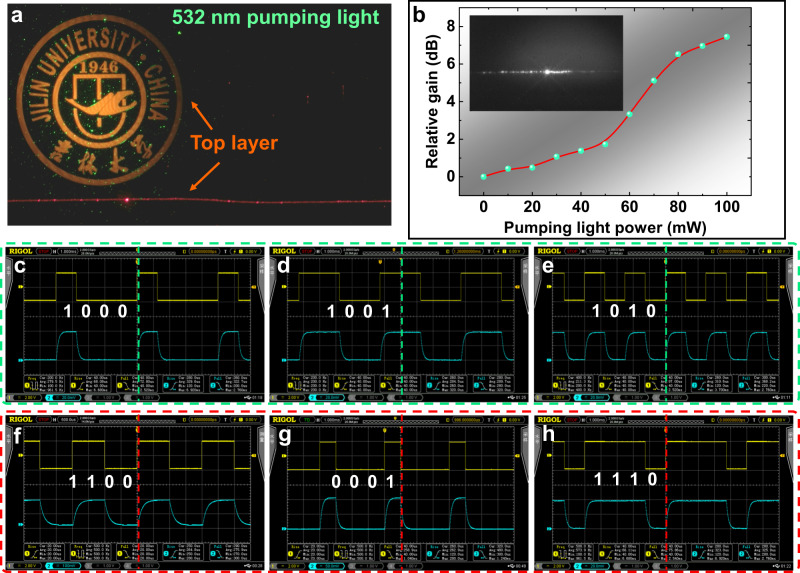
- For the encryption/pulse-code modulation demonstration, the authors report a response time of 260 μs in one test and 264 μs in the switching/warning demonstration.
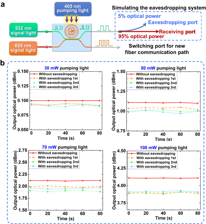
- Eavesdropping detection was tested with a 95/5 coupler; the reported average power difference was 0.13 dB, corresponding to 5.84% power splitting ratio, and the detecting accuracy reached 95.2%.
## Methods
- The study designed and fabricated a dual-layer polymer optical waveguide chip with fluorescent gain media: TCBzC (green-emitting) and TCNzC (red-emitting) doped at 5 wt‰ into SU-8; P(MMA-co-GMA) was used as the cladding/buffer material.
- Waveguide material properties were measured by ellipsometry; structures were fabricated by UV direct writing / lithography, with cross-sections examined by SEM.
- Optical testing used 532 nm and 655 nm signal sources and a 405 nm external pumping light source modulated by a digital signal generator; output spectra, gains, and response times were measured with a spectrometer, photodetector, and oscilloscope.
## Limitations
- The paper does not report a quantitative comparison against existing optical encryption chips or other encryption modalities, so the advantage over prior systems is not directly benchmarked. This is evident from the provided text.
- The discussion notes light leakage and possible refractive index perturbation from thermal stress changes in fabrication, which may affect measured outputs. This is stated/implied in the paper.
- The text does not provide long-term reliability, environmental stability, or field-deployment testing of the chip. This is not stated in the paper.
Model-written summary. Check it against the paper before relying on it.
Integrity signals
Registry
Cites
Statistics
Figures
Verification
Claims the paper makes
1 Valid · 2 Not valid · 8 Not checked · 46 Own results and interpretations
The cited sources that could be checked couldn’t confirm or dispute this claim.
In the paper
“Absorption peaks at 430 and 505 nm wavelength in visible light region are obtained37.”
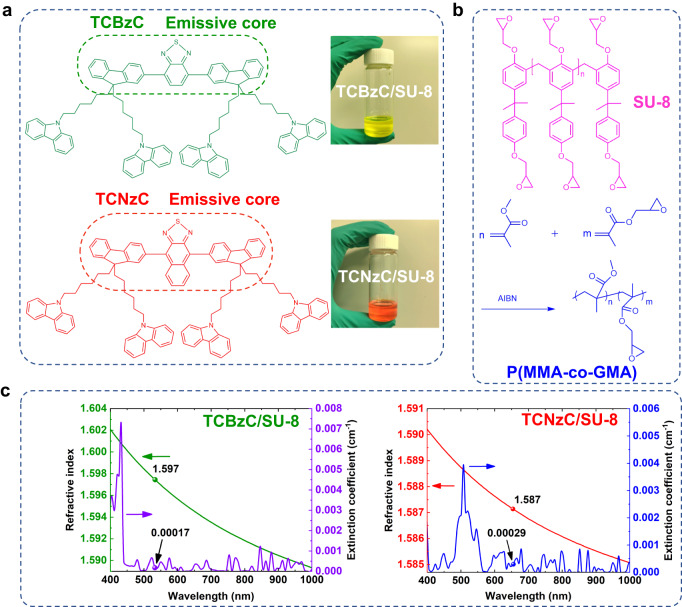
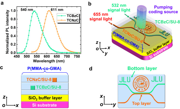
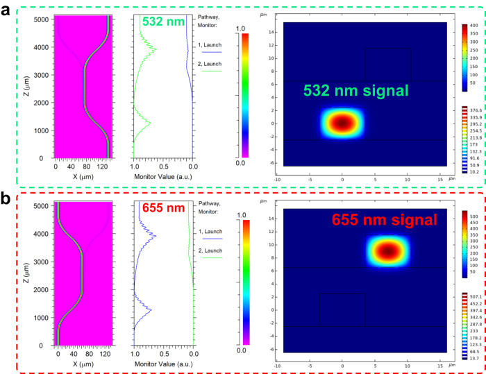
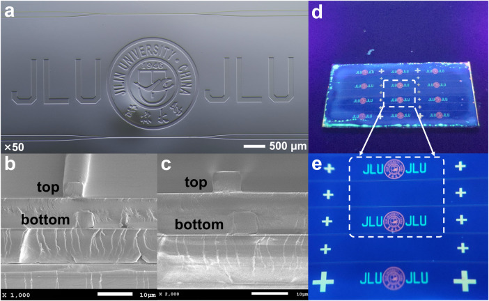
§ Dual-layer optical encryption fluorescent polymer waveguide chip based on optical pulse-code modulation technique > Results The molecular structure formulas of synthesized fluorescent small molecule oligomers green-light TCBzC and red-light TCNzC are illustrated in Fig. 1a36. This structure has several advantages. Firstly, flexible alkyl chains suspended on the main chain endow the oligomers solution processing properties. Secondly, the materials are amorphous, they do not crystallize or aggregate in the film. Meanwhile, different luminescent rigid cores (2,1,3-benzothiadiazole for TCBzC and 2,1,3-naphthalenediazole for TCNzC) are existing in the molecules, so that green and red-light emission could be achieved, respectively. In the experiment, we doped TCBzC and TCNzC with the mass fraction of 5 wt‰ in the epoxy cross-linking SU-8 polymer, respectively, to form waveguide core layer materials with better PL and gain properties. As shown in Fig. 1a, both TCBzC/SU-8 and TCNzC/SU-8 can form transparent and uniform solutions. SU-8 is an epoxy-resin type negative photoresist, and the molecular structure of SU-8 is given in Fig. 1b. The polymer material has a high exposure uniformity, and the waveguide obtained by the photolithography process has a good steepness. In addition, it has fine self-leveling ability, so that well-shaped optical waveguide patterns can be achieved. For the cladding layer material of the polymer waveguide device, we chose methyl methacrylate-propyl methacrylate epoxy copolymer (P(MMA-co-GMA)), which is an epoxy cross-linking acrylic resin material. We can synthesize it in the laboratory with methyl methacrylate (MMA) and propylene oxide methacrylate (GMA) by copolymerization, as shown in Fig. 1b. The refractive index of the self-synthesized P(MMA-co-GMA) film is 1.490 measured by an ellipsometer (SPEL M-2000VI, America) from 500 to 700 nm wavelength, which has a minor birefringence and can be adjusted in a wide range. The varied curves for refractive index (n) and extinction coefficient (k) in Vis-NIR wavelength region for TCBzC/SU-8 and TCNzC/SU-8 waveguide materials are measured by the ellipsometer. The refractive index of bottom layer waveguide material TCBzC/SU-8 is 1.597 at 532 nm wavelength and for top layer waveguide material TCNzC/SU-8 is 1.587 at 655 nm wavelength as given in Fig. 1c. According to the complex refractive index (ñ) function of ñ = n + ik, k refers to the imaginary part of the optical constant as optical absorption-loss coefficient. Therefore, the value of k could be defined as the main optical-loss coefficient for TCBzC/SU-8 and TCNzC/SU-8 waveguide materials. In Fig. 1c, it could be found that the values of k for both TCBzC/SU-8 waveguide material at 532 nm wavelength and TCNzC/SU-8 waveguide material at 655 nm wavelength are <3 × 10⁻⁴ cm−1. It is demonstrated that TCBzC/SU-8 waveguide material at 532 nm wavelength and TCNzC/SU-8 waveguide material at 655 nm wavelength have low optical-loss characterization. Moreover, multilayer waveguide devices can be easily realized by spin-coating technique, which can meet our demand for 3D integrated photonic chip. > Design and simulation of dual-layer optical encryption waveguide chip The normalized PL intensity spectra of TCBzC and TCNzC are depicted in Fig. 2a. Emission peaks as 540 and 611 nm wavelength are pumped with the 365 nm wavelength light. Absorption peaks at 430 and 505 nm wavelength in visible light region are obtained37. Based on the absorbance spectra, there should be a fluorescence energy resonance transfer (FERT) between TCBzC and TCNzC. In experiment, the dual-layer optical encryption fluorescent polymer waveguide structure is designed and fabricated. TCBzC and TCNzC are solely used as gain medium for top and bottom waveguide layer, respectively. The P(MMA-co-GMA) buffer layer between the top (TCNzC/SU-8) and bottom (TCBzC/SU-8) waveguide layers could effectively avoid the FERT phenomenon and guarantee the performances of the waveguide chip. Compared to 365 nm ultraviolet (UV) wavelength light chosen to analyze PL characteristic of the dye oligomers (TCBzC and TCNzC), 405 nm visible wavelength light is used to pump the actual waveguide chip. The main reason is that 365 nm UV wavelength light might cause photo-bleaching phenomenon for the dye oligomers in polymer waveguide. Contrast to 365 nm wavelength UV light, 405 nm visible wavelength has enough photon energy while hardly result in damage to the dye oligomers in polymer waveguide. Therefore, 405 nm visible wavelength light is used to pump the waveguide chip by optical pulse-code modulation technique in actual experiment. Accordingly, for the waveguide device fabricated by TCBzC/SU-8, with the 532 nm wavelength light as the signal light, the intensity of the output 532 nm signal light will be gained when the enhancement generated in the optical power intensity of the 405 nm pumping light. Depending on the 655 nm wavelength light as key signal source in visible light fiber communication system38,39, it might not be the maximum fluorescence emission peak of TCNzC (at 610 nm length), but there will be greatly potential application in actual optical information transmission network. When the signal light at 655 nm wavelength is coupled into the TCNzC/SU-8 waveguide with 405 or 532 nm pumping light as the external excitation source, the intensity of the signal light output from the waveguide device will also be enhanced. Based on the above, the 3D structure of a dual-layer optical encryption fluorescent polymer waveguide chip is proposed as illustrated in Fig. 2b. The cross-sectional and top-view structure of the dual-layer waveguide device are given in Figs. 2c and d, respectively. The TCBzC/SU-8 is selected as the bottom layer for optical information transmission and the abbreviation of Jilin University (JLU), with a 532 nm wavelength optical source used as the signal light. A self-synthesized P(MMA-co-GMA) polymer with high transparency and thermal stability is chosen for the upper, lower, and buffer layers of the dual-layer waveguide device. And then the TCNzC/SU-8 was used as the top waveguide layer material for the optical information transmission and the logo of Jilin University. By emitting pumping light at different power intensities at the top of the waveguide device, different types of fluorescent material doped optical waveguide will absorb the pumping light and produce gains. Based on the proposed structure of the dual-layer optical encryption waveguide, we have optimized the detailed structural sizes of the waveguide as given in Fig. 3. The cross-sectional size of the polymer waveguide core layer is 5 × 7 μm2 as displayed in Figs. 3a and b, so that the overlapping integral factor of the fundamental modes for the pumping light and signal source could reach more than 99%. The distance between the buffer layer and two waveguide layers is 4 µm, which allows the optical field to be better confined in the core layer. To couple the optical waveguide device with a commercial fiber array (Shijia Photons, G657A-1m-FC/APC), the horizontal spacings between the input and output waveguide channels for top and bottom layers are defined as 127 μm. The length of the bending waveguide is 1500 μm, and the length of the straight waveguide in the tangential section is 1150 μm. The waveguides of top and bottom layers are tangent in the vertical direction to ensure that the waveguides in both layers could absorb the pumping light energy sufficiently. After finishing the 3D structural design optimization of the dual-layer encryption waveguide device, we fabricated the device by mature semiconductor process techniques.
What the sources say
- Could not verifycites [37] Wang, C. et al. On-chip optical sources of 3D photonic integration based on active fluorescent polymer waveguide microdisks for light display application. PhotoniX 4, 13 (2023). sourceExperimental — accuracy not yet measured
Our copy reports the TCBzC/TCNzC absorbance data only as Fig. 1b ('optical absorbance and PL spectra of TCBzC and TCNzC', Fluorescent gain polymer waveguide materials) without stating any absorption peak wavelengths; the numeric peaks it does give are PL emission peaks at 540 nm and 611 nm under 365 nm excitation. Searched for '430 nm', '505 nm', absorption peak/band and absorption coefficient: the only absorption statements are that TCNzC's absorption coefficient at 532 nm is ~20 times that at 405 nm (Fabrication and testing of dual-microdisk on-chip optical sources) and that TCBzC/SU-8 has higher absorption of 405 nm pump light (single-microdisk section). No passage states or contradicts absorption peaks at 430 and 505 nm, so the claim cannot be checked against our copy. (LLM, conf=0.62)
plain- Asserted: passes — The authors put it forward as true.
- Checkable: passes — It can be checked against evidence.
- Load-bearing: passes — The paper’s conclusions depend on it.
- Based: passes — The paper gives a reason why it holds.
- Could not verify
A result the paper reports from its own data — it cites no other source for it, so there is none to check. The quote shows it is in the paper.
In the paper
“The maximum relative gains of TCBzC/SU-8 and TCNzC/SU-8 waveguide at 532 and 655 nm wavelength are 5.71 and 5.34 dB, respectively.”
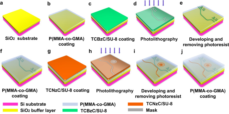
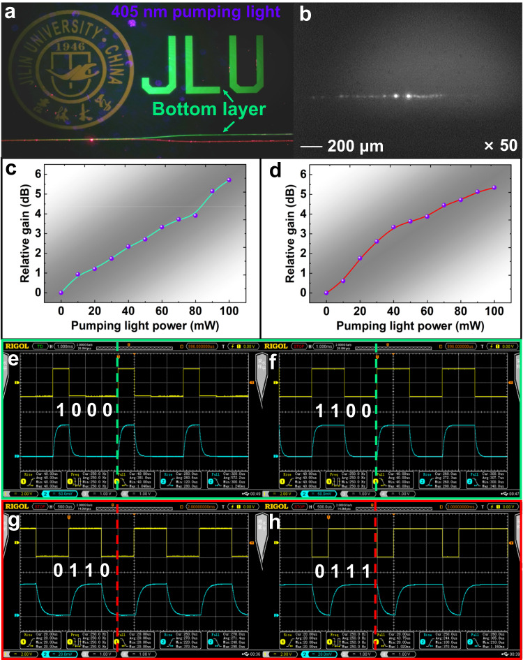
- Also stated in: § Fabrication and testing of dual-layer optical encryption waveguide chip The designed dual-layer optical encryption fluorescent polymer waveguide chip could be fabricated by UV direct written technique as given in Fig. 4. The fabrication process of the bottom waveguide layer chip was shown in Fig. 4a–f, and for the top waveguide layer was shown in Fig. 4g–j. A standard silicon wafer with the SiO2 buffer layer of 5 μm thickness was immersed in acetone and cleaned with an ultrasonic cleaner for 5 min. Then the organic solvent was removed by means of ultrasound in iso-propyl alcohol (IPA) for 5 min. After cleaning with deionized water and blow-drying with nitrogen gun, the Si substrate was dried in an oven and heated at 120 °C for 30 min as illustrated in Fig. 4a. After drying, the SiO2 substrate was prepared for the next process. Firstly, the 10 μm thickness P(MMA-co-GMA) lower cladding was spinning-coated on the SiO2 substrate as given in Fig. 4b, and then the TCBzC/SU-8 was rotated on the lower cladding layer as shown in Fig. 4c. The thickness of the waveguide core layer was formed into 5 μm by controlling the rotating speed as 3000 r/min for 30 s. The fluorescent polymer thin film was prebaked on a heating plate at 60 °C for 10 min, and then up to 90 °C for 20 min. After cooling to room temperature at 25 °C, the polymer thin film was exposed for 7 s with the lithography machine (ABM/6/350) in Fig. 4d. Then with post-baking (65 °C for 10 min, and 95 °C for 20 min), the epoxy groups in SU-8 were cross-linked at the exposed position, which can improve thermal stability. Finally, the UV written waveguide chip was immersed in photoresist developer (propylene glycol methyl ether acetate (PGMEA)) for 15 s as given in Fig. 4e. After that, the polymer thin film region without epoxy cross-linked was dissolved. It was then placed on the heating plate for hard-baking at a temperature of 120 °C for 30 min. Next, the bottom waveguide layer covered with P(MMA-co-GMA) as a buffer layer (at a speed of 3000 rpm @ 20 s) was shown in Fig. 4f. The single-layer optical encryption waveguide chip was realized as illustrated in Fig. 4a–f. For the top layer polymer waveguide chip, the fabrication process was similar to above. The TCNzC/SU-8 polymer thin film was spin-coated on the P(MMA-co-GMA) buffer layer at the speed of 3000 rpm@20 s as given in Fig. 4g. The positions of the dual-layer waveguide sidewalls were aligned during the exposure fabrication process. And the detailed operating process was the same as Fig. 4d–f. Finally, the dual-layer optical encryption fluorescent polymer waveguide chip was achieved as given in Fig. 4a–j. The dual-layer optical waveguide device was fabricated with the above process. The top view of the waveguide structure was captured as given in Fig. 5a. The structures of the dual-layer waveguide, the university logo, and JLU abbreviation doped with the different fluorescent polymers were clear and intact. The cross-sectional structure of the dual-layer waveguide was collected by a scanning electron microscopy (SEM, JSM-7900F) as shown in Fig. 5b, c. It can be seen that a clear demarcation line exists between the waveguide core and cladding layer materials, demonstrating that there is no miscibility phenomenon in different waveguide layers. In addition, the wet-etching method allows for a better shaped waveguide core layer structure. The waveguide core layer size was 7.3 × 5 μm2, which is consistent with the design dimensions. It shows that shaped core waveguide layer structures can be realized well by spin-coating and wet-etching process. This method eliminates the need for epitaxial growth techniques, dry-etching, and mask preparation, which not only greatly simplifies the fabrication process of multilayer waveguide, but also helps to reduce manufacturing costs and accelerate the speed of waveguide device fabrication. We used a 365 nm point light source to irradiate the fabricated dual-layer waveguide chip to verify the fluorescence effect, as shown in Fig. 5d. A partially enlarged photograph of the device was given in Fig. 5e. It can be clearly observed that the different fluorescent polymers can emit green and orange light, respectively, while the bottom and top layers of the aligned cross markers showed a yellow color due to the overlay of the two colors. After finishing the fabrication of the dual-layer waveguide device, the optical properties and the dynamic modulation response were then tested in order to verify its optical pulse-code modulation communication encryption performances. An optical pulse-code modulation coupling testing system was built as illustrated in Fig. S1. For the analysis of the optical gain characteristics of the dual-layer waveguide chip based on continuous-wave (CW) pumping light, we can measure the output spectra at different power pumping light with the fiber optic spectrometer (FX2000) connected to a server computer, and then the gains at different pumping light intensities could be calculated. When analyzing the optical encryption communication characteristics of the waveguide chip, the 405-nm laser was modulated as a pulse-code pumping light source. The output optical response signal from the dual-layer encryption optical waveguide device was then coupled into the photoelectric detector and converted into an electrical signal, which can be displayed on a digital oscilloscope (DS4024) for encryption modulation wave and response time testing. At the same time, the original frequency pulse-code modulation square-wave generated by the digital signal generator will be selected as a reference signal. As captured in Fig. 6a, b, the photographs were taken with vertical and horizontal CCD microscope cameras by coupling the 532 and 655 nm signal lights into the dual-layer waveguide chip with 50 mW power intensity of 405 nm pumping light as the external irradiation source. It can be noticed from Fig. 6a that the both signal lights were able to realize a stable optical beam transmission at different waveguide layers. At the same time, the university logo and the JLU abbreviation on both waveguide layers could emit the corresponding orange and green light, respectively. Furthermore, we can observe that with the same input optical power intensity, the output optical power intensity of the 532 nm signal light in the bottom TCBzC/SU-8 layer (right) is higher than that of the 655 nm signal light in the top TCNzC/SU-8 layer (left), when the pumping light was applied to the waveguide chip in Fig. 6b. The main reason for the detectable intermittent bright spots in Fig. 6b should be due to the light leakage phenomenon. It might be caused by the actual refractive index perturbation from the thermal stress change between the upper and lower cladding in fabrication process. Further, we measured the relative gains produced by different external pumping light power intensities for two different wavelengths of signal light. The relative gain is defined as:1where is the power of the waveguide output signal light when 405 nm pumping light applied, and Pout is the optical power intensity of the output signal without pumping light applied. When the input signal light wavelength was 532 nm, we have measured the relative gain of the bottom TCBzC/SU-8 waveguide layer with the pumping light power applied, when the optical power of the signal light is 30 mW, as summarized in Table 1. And the illustration drawn from the data was shown in Fig. 6c. It can be observed that when the power of the input signal light is constant, the relative gain of the measured waveguide gradually increased with the increasing in the power intensity of the external pumping light, which showed a linear growth. When the pumping light power was 100 mW, the maximum relative gain at 532 nm wavelength signal source was 5.71 dB. When the signal light wavelength was 655 nm, the increasement amplitude in relative gain decreased and flatten out as the applied external pumping light power grown. The maximum relative gain at 655 nm wavelength was 5.34 dB when the pumping light power was 100 mW, as summarized in Table 1. And the illustration from the data was shown in Fig. 6d. It can be demonstrated that the relative gain of the TCBzC/SU-8 waveguide was slightly higher than that of the TCNzC/SU-8 waveguide when the optical power of 405 nm wavelength external pumping light was equal. The optical pulse-code modulation performance can be carried out by utilizing the feature that both of fluorescent polymer top and bottom waveguides can generate relative gain at 405 nm wavelength external pumping light. The photonic plaintext digital information can be simultaneously generated by both bottom TCBzC/SU-8 waveguide layer for external optical fiber network and top TCNzC/SU-8 waveguide layer for internal optical fiber standby network. When message codes as [1000] and [1100] are output at a frequency of 250 Hz, respectively (yellow square-wave), the corresponding blue square-waves on the digital oscilloscope from the bottom TCBzC/SU-8 waveguide layer are obtained as shown in Fig. 6e, f, respectively. And the rise and fall time were measured to be 260 and 300 μs, respectively. As given in Fig. 6g, h, message codes as [0110] and [0111] are generated at the frequency of 250 Hz, respectively (yellow square-wave). The corresponding blue square-waves on the digital oscilloscope are received from the top TCNzC/SU-8 waveguide layer. And the rise and fall time were measured to be 270 and 300 μs, respectively. The rapid responsive time and comprehensive message transmission capacity demonstrated the feasibility of the waveguide device for optical pulse-code modulation encryption communication. · plain
“The maximum relative gain at 655 nm wavelength was 5.34 dB when the pumping light power was 100 mW, as summarized in Table 1.”
§ Dual-layer optical encryption fluorescent polymer waveguide chip based on optical pulse-code modulation technique > Introduction
plain- Asserted: passes — The authors put it forward as true.
- Checkable: passes — It can be checked against evidence.
- Load-bearing: passes — The paper’s conclusions depend on it.
- Based: passes — The paper gives a reason why it holds.
- Also stated in: § Fabrication and testing of dual-layer optical encryption waveguide chip The designed dual-layer optical encryption fluorescent polymer waveguide chip could be fabricated by UV direct written technique as given in Fig. 4. The fabrication process of the bottom waveguide layer chip was shown in Fig. 4a–f, and for the top waveguide layer was shown in Fig. 4g–j. A standard silicon wafer with the SiO2 buffer layer of 5 μm thickness was immersed in acetone and cleaned with an ultrasonic cleaner for 5 min. Then the organic solvent was removed by means of ultrasound in iso-propyl alcohol (IPA) for 5 min. After cleaning with deionized water and blow-drying with nitrogen gun, the Si substrate was dried in an oven and heated at 120 °C for 30 min as illustrated in Fig. 4a. After drying, the SiO2 substrate was prepared for the next process. Firstly, the 10 μm thickness P(MMA-co-GMA) lower cladding was spinning-coated on the SiO2 substrate as given in Fig. 4b, and then the TCBzC/SU-8 was rotated on the lower cladding layer as shown in Fig. 4c. The thickness of the waveguide core layer was formed into 5 μm by controlling the rotating speed as 3000 r/min for 30 s. The fluorescent polymer thin film was prebaked on a heating plate at 60 °C for 10 min, and then up to 90 °C for 20 min. After cooling to room temperature at 25 °C, the polymer thin film was exposed for 7 s with the lithography machine (ABM/6/350) in Fig. 4d. Then with post-baking (65 °C for 10 min, and 95 °C for 20 min), the epoxy groups in SU-8 were cross-linked at the exposed position, which can improve thermal stability. Finally, the UV written waveguide chip was immersed in photoresist developer (propylene glycol methyl ether acetate (PGMEA)) for 15 s as given in Fig. 4e. After that, the polymer thin film region without epoxy cross-linked was dissolved. It was then placed on the heating plate for hard-baking at a temperature of 120 °C for 30 min. Next, the bottom waveguide layer covered with P(MMA-co-GMA) as a buffer layer (at a speed of 3000 rpm @ 20 s) was shown in Fig. 4f. The single-layer optical encryption waveguide chip was realized as illustrated in Fig. 4a–f. For the top layer polymer waveguide chip, the fabrication process was similar to above. The TCNzC/SU-8 polymer thin film was spin-coated on the P(MMA-co-GMA) buffer layer at the speed of 3000 rpm@20 s as given in Fig. 4g. The positions of the dual-layer waveguide sidewalls were aligned during the exposure fabrication process. And the detailed operating process was the same as Fig. 4d–f. Finally, the dual-layer optical encryption fluorescent polymer waveguide chip was achieved as given in Fig. 4a–j. The dual-layer optical waveguide device was fabricated with the above process. The top view of the waveguide structure was captured as given in Fig. 5a. The structures of the dual-layer waveguide, the university logo, and JLU abbreviation doped with the different fluorescent polymers were clear and intact. The cross-sectional structure of the dual-layer waveguide was collected by a scanning electron microscopy (SEM, JSM-7900F) as shown in Fig. 5b, c. It can be seen that a clear demarcation line exists between the waveguide core and cladding layer materials, demonstrating that there is no miscibility phenomenon in different waveguide layers. In addition, the wet-etching method allows for a better shaped waveguide core layer structure. The waveguide core layer size was 7.3 × 5 μm2, which is consistent with the design dimensions. It shows that shaped core waveguide layer structures can be realized well by spin-coating and wet-etching process. This method eliminates the need for epitaxial growth techniques, dry-etching, and mask preparation, which not only greatly simplifies the fabrication process of multilayer waveguide, but also helps to reduce manufacturing costs and accelerate the speed of waveguide device fabrication. We used a 365 nm point light source to irradiate the fabricated dual-layer waveguide chip to verify the fluorescence effect, as shown in Fig. 5d. A partially enlarged photograph of the device was given in Fig. 5e. It can be clearly observed that the different fluorescent polymers can emit green and orange light, respectively, while the bottom and top layers of the aligned cross markers showed a yellow color due to the overlay of the two colors. After finishing the fabrication of the dual-layer waveguide device, the optical properties and the dynamic modulation response were then tested in order to verify its optical pulse-code modulation communication encryption performances. An optical pulse-code modulation coupling testing system was built as illustrated in Fig. S1. For the analysis of the optical gain characteristics of the dual-layer waveguide chip based on continuous-wave (CW) pumping light, we can measure the output spectra at different power pumping light with the fiber optic spectrometer (FX2000) connected to a server computer, and then the gains at different pumping light intensities could be calculated. When analyzing the optical encryption communication characteristics of the waveguide chip, the 405-nm laser was modulated as a pulse-code pumping light source. The output optical response signal from the dual-layer encryption optical waveguide device was then coupled into the photoelectric detector and converted into an electrical signal, which can be displayed on a digital oscilloscope (DS4024) for encryption modulation wave and response time testing. At the same time, the original frequency pulse-code modulation square-wave generated by the digital signal generator will be selected as a reference signal. As captured in Fig. 6a, b, the photographs were taken with vertical and horizontal CCD microscope cameras by coupling the 532 and 655 nm signal lights into the dual-layer waveguide chip with 50 mW power intensity of 405 nm pumping light as the external irradiation source. It can be noticed from Fig. 6a that the both signal lights were able to realize a stable optical beam transmission at different waveguide layers. At the same time, the university logo and the JLU abbreviation on both waveguide layers could emit the corresponding orange and green light, respectively. Furthermore, we can observe that with the same input optical power intensity, the output optical power intensity of the 532 nm signal light in the bottom TCBzC/SU-8 layer (right) is higher than that of the 655 nm signal light in the top TCNzC/SU-8 layer (left), when the pumping light was applied to the waveguide chip in Fig. 6b. The main reason for the detectable intermittent bright spots in Fig. 6b should be due to the light leakage phenomenon. It might be caused by the actual refractive index perturbation from the thermal stress change between the upper and lower cladding in fabrication process. Further, we measured the relative gains produced by different external pumping light power intensities for two different wavelengths of signal light. The relative gain is defined as:1where is the power of the waveguide output signal light when 405 nm pumping light applied, and Pout is the optical power intensity of the output signal without pumping light applied. When the input signal light wavelength was 532 nm, we have measured the relative gain of the bottom TCBzC/SU-8 waveguide layer with the pumping light power applied, when the optical power of the signal light is 30 mW, as summarized in Table 1. And the illustration drawn from the data was shown in Fig. 6c. It can be observed that when the power of the input signal light is constant, the relative gain of the measured waveguide gradually increased with the increasing in the power intensity of the external pumping light, which showed a linear growth. When the pumping light power was 100 mW, the maximum relative gain at 532 nm wavelength signal source was 5.71 dB. When the signal light wavelength was 655 nm, the increasement amplitude in relative gain decreased and flatten out as the applied external pumping light power grown. The maximum relative gain at 655 nm wavelength was 5.34 dB when the pumping light power was 100 mW, as summarized in Table 1. And the illustration from the data was shown in Fig. 6d. It can be demonstrated that the relative gain of the TCBzC/SU-8 waveguide was slightly higher than that of the TCNzC/SU-8 waveguide when the optical power of 405 nm wavelength external pumping light was equal. The optical pulse-code modulation performance can be carried out by utilizing the feature that both of fluorescent polymer top and bottom waveguides can generate relative gain at 405 nm wavelength external pumping light. The photonic plaintext digital information can be simultaneously generated by both bottom TCBzC/SU-8 waveguide layer for external optical fiber network and top TCNzC/SU-8 waveguide layer for internal optical fiber standby network. When message codes as [1000] and [1100] are output at a frequency of 250 Hz, respectively (yellow square-wave), the corresponding blue square-waves on the digital oscilloscope from the bottom TCBzC/SU-8 waveguide layer are obtained as shown in Fig. 6e, f, respectively. And the rise and fall time were measured to be 260 and 300 μs, respectively. As given in Fig. 6g, h, message codes as [0110] and [0111] are generated at the frequency of 250 Hz, respectively (yellow square-wave). The corresponding blue square-waves on the digital oscilloscope are received from the top TCNzC/SU-8 waveguide layer. And the rise and fall time were measured to be 270 and 300 μs, respectively. The rapid responsive time and comprehensive message transmission capacity demonstrated the feasibility of the waveguide device for optical pulse-code modulation encryption communication. · plain
A result the paper reports from its own data — it cites no other source for it, so there is none to check. The quote shows it is in the paper.
In the paper
“When the signal light wavelength was 655 nm, the increasement amplitude in relative gain decreased and flatten out as the applied external pumping light power grown.”
§ Dual-layer optical encryption fluorescent polymer waveguide chip based on optical pulse-code modulation technique > Results The molecular structure formulas of synthesized fluorescent small molecule oligomers green-light TCBzC and red-light TCNzC are illustrated in Fig. 1a36. This structure has several advantages. Firstly, flexible alkyl chains suspended on the main chain endow the oligomers solution processing properties. Secondly, the materials are amorphous, they do not crystallize or aggregate in the film. Meanwhile, different luminescent rigid cores (2,1,3-benzothiadiazole for TCBzC and 2,1,3-naphthalenediazole for TCNzC) are existing in the molecules, so that green and red-light emission could be achieved, respectively. In the experiment, we doped TCBzC and TCNzC with the mass fraction of 5 wt‰ in the epoxy cross-linking SU-8 polymer, respectively, to form waveguide core layer materials with better PL and gain properties. As shown in Fig. 1a, both TCBzC/SU-8 and TCNzC/SU-8 can form transparent and uniform solutions. SU-8 is an epoxy-resin type negative photoresist, and the molecular structure of SU-8 is given in Fig. 1b. The polymer material has a high exposure uniformity, and the waveguide obtained by the photolithography process has a good steepness. In addition, it has fine self-leveling ability, so that well-shaped optical waveguide patterns can be achieved. For the cladding layer material of the polymer waveguide device, we chose methyl methacrylate-propyl methacrylate epoxy copolymer (P(MMA-co-GMA)), which is an epoxy cross-linking acrylic resin material. We can synthesize it in the laboratory with methyl methacrylate (MMA) and propylene oxide methacrylate (GMA) by copolymerization, as shown in Fig. 1b. The refractive index of the self-synthesized P(MMA-co-GMA) film is 1.490 measured by an ellipsometer (SPEL M-2000VI, America) from 500 to 700 nm wavelength, which has a minor birefringence and can be adjusted in a wide range. The varied curves for refractive index (n) and extinction coefficient (k) in Vis-NIR wavelength region for TCBzC/SU-8 and TCNzC/SU-8 waveguide materials are measured by the ellipsometer. The refractive index of bottom layer waveguide material TCBzC/SU-8 is 1.597 at 532 nm wavelength and for top layer waveguide material TCNzC/SU-8 is 1.587 at 655 nm wavelength as given in Fig. 1c. According to the complex refractive index (ñ) function of ñ = n + ik, k refers to the imaginary part of the optical constant as optical absorption-loss coefficient. Therefore, the value of k could be defined as the main optical-loss coefficient for TCBzC/SU-8 and TCNzC/SU-8 waveguide materials. In Fig. 1c, it could be found that the values of k for both TCBzC/SU-8 waveguide material at 532 nm wavelength and TCNzC/SU-8 waveguide material at 655 nm wavelength are <3 × 10⁻⁴ cm−1. It is demonstrated that TCBzC/SU-8 waveguide material at 532 nm wavelength and TCNzC/SU-8 waveguide material at 655 nm wavelength have low optical-loss characterization. Moreover, multilayer waveguide devices can be easily realized by spin-coating technique, which can meet our demand for 3D integrated photonic chip. > Fabrication and testing of dual-layer optical encryption waveguide chip The designed dual-layer optical encryption fluorescent polymer waveguide chip could be fabricated by UV direct written technique as given in Fig. 4. The fabrication process of the bottom waveguide layer chip was shown in Fig. 4a–f, and for the top waveguide layer was shown in Fig. 4g–j. A standard silicon wafer with the SiO2 buffer layer of 5 μm thickness was immersed in acetone and cleaned with an ultrasonic cleaner for 5 min. Then the organic solvent was removed by means of ultrasound in iso-propyl alcohol (IPA) for 5 min. After cleaning with deionized water and blow-drying with nitrogen gun, the Si substrate was dried in an oven and heated at 120 °C for 30 min as illustrated in Fig. 4a. After drying, the SiO2 substrate was prepared for the next process. Firstly, the 10 μm thickness P(MMA-co-GMA) lower cladding was spinning-coated on the SiO2 substrate as given in Fig. 4b, and then the TCBzC/SU-8 was rotated on the lower cladding layer as shown in Fig. 4c. The thickness of the waveguide core layer was formed into 5 μm by controlling the rotating speed as 3000 r/min for 30 s. The fluorescent polymer thin film was prebaked on a heating plate at 60 °C for 10 min, and then up to 90 °C for 20 min. After cooling to room temperature at 25 °C, the polymer thin film was exposed for 7 s with the lithography machine (ABM/6/350) in Fig. 4d. Then with post-baking (65 °C for 10 min, and 95 °C for 20 min), the epoxy groups in SU-8 were cross-linked at the exposed position, which can improve thermal stability. Finally, the UV written waveguide chip was immersed in photoresist developer (propylene glycol methyl ether acetate (PGMEA)) for 15 s as given in Fig. 4e. After that, the polymer thin film region without epoxy cross-linked was dissolved. It was then placed on the heating plate for hard-baking at a temperature of 120 °C for 30 min. Next, the bottom waveguide layer covered with P(MMA-co-GMA) as a buffer layer (at a speed of 3000 rpm @ 20 s) was shown in Fig. 4f. The single-layer optical encryption waveguide chip was realized as illustrated in Fig. 4a–f. For the top layer polymer waveguide chip, the fabrication process was similar to above. The TCNzC/SU-8 polymer thin film was spin-coated on the P(MMA-co-GMA) buffer layer at the speed of 3000 rpm@20 s as given in Fig. 4g. The positions of the dual-layer waveguide sidewalls were aligned during the exposure fabrication process. And the detailed operating process was the same as Fig. 4d–f. Finally, the dual-layer optical encryption fluorescent polymer waveguide chip was achieved as given in Fig. 4a–j. The dual-layer optical waveguide device was fabricated with the above process. The top view of the waveguide structure was captured as given in Fig. 5a. The structures of the dual-layer waveguide, the university logo, and JLU abbreviation doped with the different fluorescent polymers were clear and intact. The cross-sectional structure of the dual-layer waveguide was collected by a scanning electron microscopy (SEM, JSM-7900F) as shown in Fig. 5b, c. It can be seen that a clear demarcation line exists between the waveguide core and cladding layer materials, demonstrating that there is no miscibility phenomenon in different waveguide layers. In addition, the wet-etching method allows for a better shaped waveguide core layer structure. The waveguide core layer size was 7.3 × 5 μm2, which is consistent with the design dimensions. It shows that shaped core waveguide layer structures can be realized well by spin-coating and wet-etching process. This method eliminates the need for epitaxial growth techniques, dry-etching, and mask preparation, which not only greatly simplifies the fabrication process of multilayer waveguide, but also helps to reduce manufacturing costs and accelerate the speed of waveguide device fabrication. We used a 365 nm point light source to irradiate the fabricated dual-layer waveguide chip to verify the fluorescence effect, as shown in Fig. 5d. A partially enlarged photograph of the device was given in Fig. 5e. It can be clearly observed that the different fluorescent polymers can emit green and orange light, respectively, while the bottom and top layers of the aligned cross markers showed a yellow color due to the overlay of the two colors. After finishing the fabrication of the dual-layer waveguide device, the optical properties and the dynamic modulation response were then tested in order to verify its optical pulse-code modulation communication encryption performances. An optical pulse-code modulation coupling testing system was built as illustrated in Fig. S1. For the analysis of the optical gain characteristics of the dual-layer waveguide chip based on continuous-wave (CW) pumping light, we can measure the output spectra at different power pumping light with the fiber optic spectrometer (FX2000) connected to a server computer, and then the gains at different pumping light intensities could be calculated. When analyzing the optical encryption communication characteristics of the waveguide chip, the 405-nm laser was modulated as a pulse-code pumping light source. The output optical response signal from the dual-layer encryption optical waveguide device was then coupled into the photoelectric detector and converted into an electrical signal, which can be displayed on a digital oscilloscope (DS4024) for encryption modulation wave and response time testing. At the same time, the original frequency pulse-code modulation square-wave generated by the digital signal generator will be selected as a reference signal. As captured in Fig. 6a, b, the photographs were taken with vertical and horizontal CCD microscope cameras by coupling the 532 and 655 nm signal lights into the dual-layer waveguide chip with 50 mW power intensity of 405 nm pumping light as the external irradiation source. It can be noticed from Fig. 6a that the both signal lights were able to realize a stable optical beam transmission at different waveguide layers. At the same time, the university logo and the JLU abbreviation on both waveguide layers could emit the corresponding orange and green light, respectively. Furthermore, we can observe that with the same input optical power intensity, the output optical power intensity of the 532 nm signal light in the bottom TCBzC/SU-8 layer (right) is higher than that of the 655 nm signal light in the top TCNzC/SU-8 layer (left), when the pumping light was applied to the waveguide chip in Fig. 6b. The main reason for the detectable intermittent bright spots in Fig. 6b should be due to the light leakage phenomenon. It might be caused by the actual refractive index perturbation from the thermal stress change between the upper and lower cladding in fabrication process. Further, we measured the relative gains produced by different external pumping light power intensities for two different wavelengths of signal light. The relative gain is defined as:1where is the power of the waveguide output signal light when 405 nm pumping light applied, and Pout is the optical power intensity of the output signal without pumping light applied. When the input signal light wavelength was 532 nm, we have measured the relative gain of the bottom TCBzC/SU-8 waveguide layer with the pumping light power applied, when the optical power of the signal light is 30 mW, as summarized in Table 1. And the illustration drawn from the data was shown in Fig. 6c. It can be observed that when the power of the input signal light is constant, the relative gain of the measured waveguide gradually increased with the increasing in the power intensity of the external pumping light, which showed a linear growth. When the pumping light power was 100 mW, the maximum relative gain at 532 nm wavelength signal source was 5.71 dB. When the signal light wavelength was 655 nm, the increasement amplitude in relative gain decreased and flatten out as the applied external pumping light power grown. The maximum relative gain at 655 nm wavelength was 5.34 dB when the pumping light power was 100 mW, as summarized in Table 1. And the illustration from the data was shown in Fig. 6d. It can be demonstrated that the relative gain of the TCBzC/SU-8 waveguide was slightly higher than that of the TCNzC/SU-8 waveguide when the optical power of 405 nm wavelength external pumping light was equal. The optical pulse-code modulation performance can be carried out by utilizing the feature that both of fluorescent polymer top and bottom waveguides can generate relative gain at 405 nm wavelength external pumping light. The photonic plaintext digital information can be simultaneously generated by both bottom TCBzC/SU-8 waveguide layer for external optical fiber network and top TCNzC/SU-8 waveguide layer for internal optical fiber standby network. When message codes as [1000] and [1100] are output at a frequency of 250 Hz, respectively (yellow square-wave), the corresponding blue square-waves on the digital oscilloscope from the bottom TCBzC/SU-8 waveguide layer are obtained as shown in Fig. 6e, f, respectively. And the rise and fall time were measured to be 260 and 300 μs, respectively. As given in Fig. 6g, h, message codes as [0110] and [0111] are generated at the frequency of 250 Hz, respectively (yellow square-wave). The corresponding blue square-waves on the digital oscilloscope are received from the top TCNzC/SU-8 waveguide layer. And the rise and fall time were measured to be 270 and 300 μs, respectively. The rapid responsive time and comprehensive message transmission capacity demonstrated the feasibility of the waveguide device for optical pulse-code modulation encryption communication.
plainstates a cause- Asserted: passes — The authors put it forward as true.
- Checkable: passes — It can be checked against evidence.
- Load-bearing: unclear — It is unclear whether the paper’s conclusions depend on it.
- Based: passes — The paper gives a reason why it holds.
A result the paper reports from its own data — it cites no other source for it, so there is none to check. The quote shows it is in the paper.
In the paper
“The maximum relative gains of TCBzC/SU-8 and TCNzC/SU-8 waveguide at 532 and 655 nm wavelength are 5.71 and 5.34 dB, respectively.”
- Also stated in: § Fabrication and testing of dual-layer optical encryption waveguide chip The designed dual-layer optical encryption fluorescent polymer waveguide chip could be fabricated by UV direct written technique as given in Fig. 4. The fabrication process of the bottom waveguide layer chip was shown in Fig. 4a–f, and for the top waveguide layer was shown in Fig. 4g–j. A standard silicon wafer with the SiO2 buffer layer of 5 μm thickness was immersed in acetone and cleaned with an ultrasonic cleaner for 5 min. Then the organic solvent was removed by means of ultrasound in iso-propyl alcohol (IPA) for 5 min. After cleaning with deionized water and blow-drying with nitrogen gun, the Si substrate was dried in an oven and heated at 120 °C for 30 min as illustrated in Fig. 4a. After drying, the SiO2 substrate was prepared for the next process. Firstly, the 10 μm thickness P(MMA-co-GMA) lower cladding was spinning-coated on the SiO2 substrate as given in Fig. 4b, and then the TCBzC/SU-8 was rotated on the lower cladding layer as shown in Fig. 4c. The thickness of the waveguide core layer was formed into 5 μm by controlling the rotating speed as 3000 r/min for 30 s. The fluorescent polymer thin film was prebaked on a heating plate at 60 °C for 10 min, and then up to 90 °C for 20 min. After cooling to room temperature at 25 °C, the polymer thin film was exposed for 7 s with the lithography machine (ABM/6/350) in Fig. 4d. Then with post-baking (65 °C for 10 min, and 95 °C for 20 min), the epoxy groups in SU-8 were cross-linked at the exposed position, which can improve thermal stability. Finally, the UV written waveguide chip was immersed in photoresist developer (propylene glycol methyl ether acetate (PGMEA)) for 15 s as given in Fig. 4e. After that, the polymer thin film region without epoxy cross-linked was dissolved. It was then placed on the heating plate for hard-baking at a temperature of 120 °C for 30 min. Next, the bottom waveguide layer covered with P(MMA-co-GMA) as a buffer layer (at a speed of 3000 rpm @ 20 s) was shown in Fig. 4f. The single-layer optical encryption waveguide chip was realized as illustrated in Fig. 4a–f. For the top layer polymer waveguide chip, the fabrication process was similar to above. The TCNzC/SU-8 polymer thin film was spin-coated on the P(MMA-co-GMA) buffer layer at the speed of 3000 rpm@20 s as given in Fig. 4g. The positions of the dual-layer waveguide sidewalls were aligned during the exposure fabrication process. And the detailed operating process was the same as Fig. 4d–f. Finally, the dual-layer optical encryption fluorescent polymer waveguide chip was achieved as given in Fig. 4a–j. The dual-layer optical waveguide device was fabricated with the above process. The top view of the waveguide structure was captured as given in Fig. 5a. The structures of the dual-layer waveguide, the university logo, and JLU abbreviation doped with the different fluorescent polymers were clear and intact. The cross-sectional structure of the dual-layer waveguide was collected by a scanning electron microscopy (SEM, JSM-7900F) as shown in Fig. 5b, c. It can be seen that a clear demarcation line exists between the waveguide core and cladding layer materials, demonstrating that there is no miscibility phenomenon in different waveguide layers. In addition, the wet-etching method allows for a better shaped waveguide core layer structure. The waveguide core layer size was 7.3 × 5 μm2, which is consistent with the design dimensions. It shows that shaped core waveguide layer structures can be realized well by spin-coating and wet-etching process. This method eliminates the need for epitaxial growth techniques, dry-etching, and mask preparation, which not only greatly simplifies the fabrication process of multilayer waveguide, but also helps to reduce manufacturing costs and accelerate the speed of waveguide device fabrication. We used a 365 nm point light source to irradiate the fabricated dual-layer waveguide chip to verify the fluorescence effect, as shown in Fig. 5d. A partially enlarged photograph of the device was given in Fig. 5e. It can be clearly observed that the different fluorescent polymers can emit green and orange light, respectively, while the bottom and top layers of the aligned cross markers showed a yellow color due to the overlay of the two colors. After finishing the fabrication of the dual-layer waveguide device, the optical properties and the dynamic modulation response were then tested in order to verify its optical pulse-code modulation communication encryption performances. An optical pulse-code modulation coupling testing system was built as illustrated in Fig. S1. For the analysis of the optical gain characteristics of the dual-layer waveguide chip based on continuous-wave (CW) pumping light, we can measure the output spectra at different power pumping light with the fiber optic spectrometer (FX2000) connected to a server computer, and then the gains at different pumping light intensities could be calculated. When analyzing the optical encryption communication characteristics of the waveguide chip, the 405-nm laser was modulated as a pulse-code pumping light source. The output optical response signal from the dual-layer encryption optical waveguide device was then coupled into the photoelectric detector and converted into an electrical signal, which can be displayed on a digital oscilloscope (DS4024) for encryption modulation wave and response time testing. At the same time, the original frequency pulse-code modulation square-wave generated by the digital signal generator will be selected as a reference signal. As captured in Fig. 6a, b, the photographs were taken with vertical and horizontal CCD microscope cameras by coupling the 532 and 655 nm signal lights into the dual-layer waveguide chip with 50 mW power intensity of 405 nm pumping light as the external irradiation source. It can be noticed from Fig. 6a that the both signal lights were able to realize a stable optical beam transmission at different waveguide layers. At the same time, the university logo and the JLU abbreviation on both waveguide layers could emit the corresponding orange and green light, respectively. Furthermore, we can observe that with the same input optical power intensity, the output optical power intensity of the 532 nm signal light in the bottom TCBzC/SU-8 layer (right) is higher than that of the 655 nm signal light in the top TCNzC/SU-8 layer (left), when the pumping light was applied to the waveguide chip in Fig. 6b. The main reason for the detectable intermittent bright spots in Fig. 6b should be due to the light leakage phenomenon. It might be caused by the actual refractive index perturbation from the thermal stress change between the upper and lower cladding in fabrication process. Further, we measured the relative gains produced by different external pumping light power intensities for two different wavelengths of signal light. The relative gain is defined as:1where is the power of the waveguide output signal light when 405 nm pumping light applied, and Pout is the optical power intensity of the output signal without pumping light applied. When the input signal light wavelength was 532 nm, we have measured the relative gain of the bottom TCBzC/SU-8 waveguide layer with the pumping light power applied, when the optical power of the signal light is 30 mW, as summarized in Table 1. And the illustration drawn from the data was shown in Fig. 6c. It can be observed that when the power of the input signal light is constant, the relative gain of the measured waveguide gradually increased with the increasing in the power intensity of the external pumping light, which showed a linear growth. When the pumping light power was 100 mW, the maximum relative gain at 532 nm wavelength signal source was 5.71 dB. When the signal light wavelength was 655 nm, the increasement amplitude in relative gain decreased and flatten out as the applied external pumping light power grown. The maximum relative gain at 655 nm wavelength was 5.34 dB when the pumping light power was 100 mW, as summarized in Table 1. And the illustration from the data was shown in Fig. 6d. It can be demonstrated that the relative gain of the TCBzC/SU-8 waveguide was slightly higher than that of the TCNzC/SU-8 waveguide when the optical power of 405 nm wavelength external pumping light was equal. The optical pulse-code modulation performance can be carried out by utilizing the feature that both of fluorescent polymer top and bottom waveguides can generate relative gain at 405 nm wavelength external pumping light. The photonic plaintext digital information can be simultaneously generated by both bottom TCBzC/SU-8 waveguide layer for external optical fiber network and top TCNzC/SU-8 waveguide layer for internal optical fiber standby network. When message codes as [1000] and [1100] are output at a frequency of 250 Hz, respectively (yellow square-wave), the corresponding blue square-waves on the digital oscilloscope from the bottom TCBzC/SU-8 waveguide layer are obtained as shown in Fig. 6e, f, respectively. And the rise and fall time were measured to be 260 and 300 μs, respectively. As given in Fig. 6g, h, message codes as [0110] and [0111] are generated at the frequency of 250 Hz, respectively (yellow square-wave). The corresponding blue square-waves on the digital oscilloscope are received from the top TCNzC/SU-8 waveguide layer. And the rise and fall time were measured to be 270 and 300 μs, respectively. The rapid responsive time and comprehensive message transmission capacity demonstrated the feasibility of the waveguide device for optical pulse-code modulation encryption communication. · plain
“When the pumping light power was 100 mW, the maximum relative gain at 532 nm wavelength signal source was 5.71 dB.”
- Also stated in: § Outlook · plain
“the relative gain of 532 nm wavelength signal source at 100 mW of 405 nm pumping light was 5.71 dB”
§ Dual-layer optical encryption fluorescent polymer waveguide chip based on optical pulse-code modulation technique > Introduction
plain- Asserted: passes — The authors put it forward as true.
- Checkable: passes — It can be checked against evidence.
- Load-bearing: passes — The paper’s conclusions depend on it.
- Based: passes — The paper gives a reason why it holds.
- Also stated in: § Fabrication and testing of dual-layer optical encryption waveguide chip The designed dual-layer optical encryption fluorescent polymer waveguide chip could be fabricated by UV direct written technique as given in Fig. 4. The fabrication process of the bottom waveguide layer chip was shown in Fig. 4a–f, and for the top waveguide layer was shown in Fig. 4g–j. A standard silicon wafer with the SiO2 buffer layer of 5 μm thickness was immersed in acetone and cleaned with an ultrasonic cleaner for 5 min. Then the organic solvent was removed by means of ultrasound in iso-propyl alcohol (IPA) for 5 min. After cleaning with deionized water and blow-drying with nitrogen gun, the Si substrate was dried in an oven and heated at 120 °C for 30 min as illustrated in Fig. 4a. After drying, the SiO2 substrate was prepared for the next process. Firstly, the 10 μm thickness P(MMA-co-GMA) lower cladding was spinning-coated on the SiO2 substrate as given in Fig. 4b, and then the TCBzC/SU-8 was rotated on the lower cladding layer as shown in Fig. 4c. The thickness of the waveguide core layer was formed into 5 μm by controlling the rotating speed as 3000 r/min for 30 s. The fluorescent polymer thin film was prebaked on a heating plate at 60 °C for 10 min, and then up to 90 °C for 20 min. After cooling to room temperature at 25 °C, the polymer thin film was exposed for 7 s with the lithography machine (ABM/6/350) in Fig. 4d. Then with post-baking (65 °C for 10 min, and 95 °C for 20 min), the epoxy groups in SU-8 were cross-linked at the exposed position, which can improve thermal stability. Finally, the UV written waveguide chip was immersed in photoresist developer (propylene glycol methyl ether acetate (PGMEA)) for 15 s as given in Fig. 4e. After that, the polymer thin film region without epoxy cross-linked was dissolved. It was then placed on the heating plate for hard-baking at a temperature of 120 °C for 30 min. Next, the bottom waveguide layer covered with P(MMA-co-GMA) as a buffer layer (at a speed of 3000 rpm @ 20 s) was shown in Fig. 4f. The single-layer optical encryption waveguide chip was realized as illustrated in Fig. 4a–f. For the top layer polymer waveguide chip, the fabrication process was similar to above. The TCNzC/SU-8 polymer thin film was spin-coated on the P(MMA-co-GMA) buffer layer at the speed of 3000 rpm@20 s as given in Fig. 4g. The positions of the dual-layer waveguide sidewalls were aligned during the exposure fabrication process. And the detailed operating process was the same as Fig. 4d–f. Finally, the dual-layer optical encryption fluorescent polymer waveguide chip was achieved as given in Fig. 4a–j. The dual-layer optical waveguide device was fabricated with the above process. The top view of the waveguide structure was captured as given in Fig. 5a. The structures of the dual-layer waveguide, the university logo, and JLU abbreviation doped with the different fluorescent polymers were clear and intact. The cross-sectional structure of the dual-layer waveguide was collected by a scanning electron microscopy (SEM, JSM-7900F) as shown in Fig. 5b, c. It can be seen that a clear demarcation line exists between the waveguide core and cladding layer materials, demonstrating that there is no miscibility phenomenon in different waveguide layers. In addition, the wet-etching method allows for a better shaped waveguide core layer structure. The waveguide core layer size was 7.3 × 5 μm2, which is consistent with the design dimensions. It shows that shaped core waveguide layer structures can be realized well by spin-coating and wet-etching process. This method eliminates the need for epitaxial growth techniques, dry-etching, and mask preparation, which not only greatly simplifies the fabrication process of multilayer waveguide, but also helps to reduce manufacturing costs and accelerate the speed of waveguide device fabrication. We used a 365 nm point light source to irradiate the fabricated dual-layer waveguide chip to verify the fluorescence effect, as shown in Fig. 5d. A partially enlarged photograph of the device was given in Fig. 5e. It can be clearly observed that the different fluorescent polymers can emit green and orange light, respectively, while the bottom and top layers of the aligned cross markers showed a yellow color due to the overlay of the two colors. After finishing the fabrication of the dual-layer waveguide device, the optical properties and the dynamic modulation response were then tested in order to verify its optical pulse-code modulation communication encryption performances. An optical pulse-code modulation coupling testing system was built as illustrated in Fig. S1. For the analysis of the optical gain characteristics of the dual-layer waveguide chip based on continuous-wave (CW) pumping light, we can measure the output spectra at different power pumping light with the fiber optic spectrometer (FX2000) connected to a server computer, and then the gains at different pumping light intensities could be calculated. When analyzing the optical encryption communication characteristics of the waveguide chip, the 405-nm laser was modulated as a pulse-code pumping light source. The output optical response signal from the dual-layer encryption optical waveguide device was then coupled into the photoelectric detector and converted into an electrical signal, which can be displayed on a digital oscilloscope (DS4024) for encryption modulation wave and response time testing. At the same time, the original frequency pulse-code modulation square-wave generated by the digital signal generator will be selected as a reference signal. As captured in Fig. 6a, b, the photographs were taken with vertical and horizontal CCD microscope cameras by coupling the 532 and 655 nm signal lights into the dual-layer waveguide chip with 50 mW power intensity of 405 nm pumping light as the external irradiation source. It can be noticed from Fig. 6a that the both signal lights were able to realize a stable optical beam transmission at different waveguide layers. At the same time, the university logo and the JLU abbreviation on both waveguide layers could emit the corresponding orange and green light, respectively. Furthermore, we can observe that with the same input optical power intensity, the output optical power intensity of the 532 nm signal light in the bottom TCBzC/SU-8 layer (right) is higher than that of the 655 nm signal light in the top TCNzC/SU-8 layer (left), when the pumping light was applied to the waveguide chip in Fig. 6b. The main reason for the detectable intermittent bright spots in Fig. 6b should be due to the light leakage phenomenon. It might be caused by the actual refractive index perturbation from the thermal stress change between the upper and lower cladding in fabrication process. Further, we measured the relative gains produced by different external pumping light power intensities for two different wavelengths of signal light. The relative gain is defined as:1where is the power of the waveguide output signal light when 405 nm pumping light applied, and Pout is the optical power intensity of the output signal without pumping light applied. When the input signal light wavelength was 532 nm, we have measured the relative gain of the bottom TCBzC/SU-8 waveguide layer with the pumping light power applied, when the optical power of the signal light is 30 mW, as summarized in Table 1. And the illustration drawn from the data was shown in Fig. 6c. It can be observed that when the power of the input signal light is constant, the relative gain of the measured waveguide gradually increased with the increasing in the power intensity of the external pumping light, which showed a linear growth. When the pumping light power was 100 mW, the maximum relative gain at 532 nm wavelength signal source was 5.71 dB. When the signal light wavelength was 655 nm, the increasement amplitude in relative gain decreased and flatten out as the applied external pumping light power grown. The maximum relative gain at 655 nm wavelength was 5.34 dB when the pumping light power was 100 mW, as summarized in Table 1. And the illustration from the data was shown in Fig. 6d. It can be demonstrated that the relative gain of the TCBzC/SU-8 waveguide was slightly higher than that of the TCNzC/SU-8 waveguide when the optical power of 405 nm wavelength external pumping light was equal. The optical pulse-code modulation performance can be carried out by utilizing the feature that both of fluorescent polymer top and bottom waveguides can generate relative gain at 405 nm wavelength external pumping light. The photonic plaintext digital information can be simultaneously generated by both bottom TCBzC/SU-8 waveguide layer for external optical fiber network and top TCNzC/SU-8 waveguide layer for internal optical fiber standby network. When message codes as [1000] and [1100] are output at a frequency of 250 Hz, respectively (yellow square-wave), the corresponding blue square-waves on the digital oscilloscope from the bottom TCBzC/SU-8 waveguide layer are obtained as shown in Fig. 6e, f, respectively. And the rise and fall time were measured to be 260 and 300 μs, respectively. As given in Fig. 6g, h, message codes as [0110] and [0111] are generated at the frequency of 250 Hz, respectively (yellow square-wave). The corresponding blue square-waves on the digital oscilloscope are received from the top TCNzC/SU-8 waveguide layer. And the rise and fall time were measured to be 270 and 300 μs, respectively. The rapid responsive time and comprehensive message transmission capacity demonstrated the feasibility of the waveguide device for optical pulse-code modulation encryption communication. · plain
A result the paper reports from its own data — it cites no other source for it, so there is none to check. The quote shows it is in the paper.
In the paper
“It can be observed that when the power of the input signal light is constant, the relative gain of the measured waveguide gradually increased with the increasing in the power intensity of the external pumping light, which showed a linear growth.”
§ Dual-layer optical encryption fluorescent polymer waveguide chip based on optical pulse-code modulation technique > Results The molecular structure formulas of synthesized fluorescent small molecule oligomers green-light TCBzC and red-light TCNzC are illustrated in Fig. 1a36. This structure has several advantages. Firstly, flexible alkyl chains suspended on the main chain endow the oligomers solution processing properties. Secondly, the materials are amorphous, they do not crystallize or aggregate in the film. Meanwhile, different luminescent rigid cores (2,1,3-benzothiadiazole for TCBzC and 2,1,3-naphthalenediazole for TCNzC) are existing in the molecules, so that green and red-light emission could be achieved, respectively. In the experiment, we doped TCBzC and TCNzC with the mass fraction of 5 wt‰ in the epoxy cross-linking SU-8 polymer, respectively, to form waveguide core layer materials with better PL and gain properties. As shown in Fig. 1a, both TCBzC/SU-8 and TCNzC/SU-8 can form transparent and uniform solutions. SU-8 is an epoxy-resin type negative photoresist, and the molecular structure of SU-8 is given in Fig. 1b. The polymer material has a high exposure uniformity, and the waveguide obtained by the photolithography process has a good steepness. In addition, it has fine self-leveling ability, so that well-shaped optical waveguide patterns can be achieved. For the cladding layer material of the polymer waveguide device, we chose methyl methacrylate-propyl methacrylate epoxy copolymer (P(MMA-co-GMA)), which is an epoxy cross-linking acrylic resin material. We can synthesize it in the laboratory with methyl methacrylate (MMA) and propylene oxide methacrylate (GMA) by copolymerization, as shown in Fig. 1b. The refractive index of the self-synthesized P(MMA-co-GMA) film is 1.490 measured by an ellipsometer (SPEL M-2000VI, America) from 500 to 700 nm wavelength, which has a minor birefringence and can be adjusted in a wide range. The varied curves for refractive index (n) and extinction coefficient (k) in Vis-NIR wavelength region for TCBzC/SU-8 and TCNzC/SU-8 waveguide materials are measured by the ellipsometer. The refractive index of bottom layer waveguide material TCBzC/SU-8 is 1.597 at 532 nm wavelength and for top layer waveguide material TCNzC/SU-8 is 1.587 at 655 nm wavelength as given in Fig. 1c. According to the complex refractive index (ñ) function of ñ = n + ik, k refers to the imaginary part of the optical constant as optical absorption-loss coefficient. Therefore, the value of k could be defined as the main optical-loss coefficient for TCBzC/SU-8 and TCNzC/SU-8 waveguide materials. In Fig. 1c, it could be found that the values of k for both TCBzC/SU-8 waveguide material at 532 nm wavelength and TCNzC/SU-8 waveguide material at 655 nm wavelength are <3 × 10⁻⁴ cm−1. It is demonstrated that TCBzC/SU-8 waveguide material at 532 nm wavelength and TCNzC/SU-8 waveguide material at 655 nm wavelength have low optical-loss characterization. Moreover, multilayer waveguide devices can be easily realized by spin-coating technique, which can meet our demand for 3D integrated photonic chip. > Fabrication and testing of dual-layer optical encryption waveguide chip The designed dual-layer optical encryption fluorescent polymer waveguide chip could be fabricated by UV direct written technique as given in Fig. 4. The fabrication process of the bottom waveguide layer chip was shown in Fig. 4a–f, and for the top waveguide layer was shown in Fig. 4g–j. A standard silicon wafer with the SiO2 buffer layer of 5 μm thickness was immersed in acetone and cleaned with an ultrasonic cleaner for 5 min. Then the organic solvent was removed by means of ultrasound in iso-propyl alcohol (IPA) for 5 min. After cleaning with deionized water and blow-drying with nitrogen gun, the Si substrate was dried in an oven and heated at 120 °C for 30 min as illustrated in Fig. 4a. After drying, the SiO2 substrate was prepared for the next process. Firstly, the 10 μm thickness P(MMA-co-GMA) lower cladding was spinning-coated on the SiO2 substrate as given in Fig. 4b, and then the TCBzC/SU-8 was rotated on the lower cladding layer as shown in Fig. 4c. The thickness of the waveguide core layer was formed into 5 μm by controlling the rotating speed as 3000 r/min for 30 s. The fluorescent polymer thin film was prebaked on a heating plate at 60 °C for 10 min, and then up to 90 °C for 20 min. After cooling to room temperature at 25 °C, the polymer thin film was exposed for 7 s with the lithography machine (ABM/6/350) in Fig. 4d. Then with post-baking (65 °C for 10 min, and 95 °C for 20 min), the epoxy groups in SU-8 were cross-linked at the exposed position, which can improve thermal stability. Finally, the UV written waveguide chip was immersed in photoresist developer (propylene glycol methyl ether acetate (PGMEA)) for 15 s as given in Fig. 4e. After that, the polymer thin film region without epoxy cross-linked was dissolved. It was then placed on the heating plate for hard-baking at a temperature of 120 °C for 30 min. Next, the bottom waveguide layer covered with P(MMA-co-GMA) as a buffer layer (at a speed of 3000 rpm @ 20 s) was shown in Fig. 4f. The single-layer optical encryption waveguide chip was realized as illustrated in Fig. 4a–f. For the top layer polymer waveguide chip, the fabrication process was similar to above. The TCNzC/SU-8 polymer thin film was spin-coated on the P(MMA-co-GMA) buffer layer at the speed of 3000 rpm@20 s as given in Fig. 4g. The positions of the dual-layer waveguide sidewalls were aligned during the exposure fabrication process. And the detailed operating process was the same as Fig. 4d–f. Finally, the dual-layer optical encryption fluorescent polymer waveguide chip was achieved as given in Fig. 4a–j. The dual-layer optical waveguide device was fabricated with the above process. The top view of the waveguide structure was captured as given in Fig. 5a. The structures of the dual-layer waveguide, the university logo, and JLU abbreviation doped with the different fluorescent polymers were clear and intact. The cross-sectional structure of the dual-layer waveguide was collected by a scanning electron microscopy (SEM, JSM-7900F) as shown in Fig. 5b, c. It can be seen that a clear demarcation line exists between the waveguide core and cladding layer materials, demonstrating that there is no miscibility phenomenon in different waveguide layers. In addition, the wet-etching method allows for a better shaped waveguide core layer structure. The waveguide core layer size was 7.3 × 5 μm2, which is consistent with the design dimensions. It shows that shaped core waveguide layer structures can be realized well by spin-coating and wet-etching process. This method eliminates the need for epitaxial growth techniques, dry-etching, and mask preparation, which not only greatly simplifies the fabrication process of multilayer waveguide, but also helps to reduce manufacturing costs and accelerate the speed of waveguide device fabrication. We used a 365 nm point light source to irradiate the fabricated dual-layer waveguide chip to verify the fluorescence effect, as shown in Fig. 5d. A partially enlarged photograph of the device was given in Fig. 5e. It can be clearly observed that the different fluorescent polymers can emit green and orange light, respectively, while the bottom and top layers of the aligned cross markers showed a yellow color due to the overlay of the two colors. After finishing the fabrication of the dual-layer waveguide device, the optical properties and the dynamic modulation response were then tested in order to verify its optical pulse-code modulation communication encryption performances. An optical pulse-code modulation coupling testing system was built as illustrated in Fig. S1. For the analysis of the optical gain characteristics of the dual-layer waveguide chip based on continuous-wave (CW) pumping light, we can measure the output spectra at different power pumping light with the fiber optic spectrometer (FX2000) connected to a server computer, and then the gains at different pumping light intensities could be calculated. When analyzing the optical encryption communication characteristics of the waveguide chip, the 405-nm laser was modulated as a pulse-code pumping light source. The output optical response signal from the dual-layer encryption optical waveguide device was then coupled into the photoelectric detector and converted into an electrical signal, which can be displayed on a digital oscilloscope (DS4024) for encryption modulation wave and response time testing. At the same time, the original frequency pulse-code modulation square-wave generated by the digital signal generator will be selected as a reference signal. As captured in Fig. 6a, b, the photographs were taken with vertical and horizontal CCD microscope cameras by coupling the 532 and 655 nm signal lights into the dual-layer waveguide chip with 50 mW power intensity of 405 nm pumping light as the external irradiation source. It can be noticed from Fig. 6a that the both signal lights were able to realize a stable optical beam transmission at different waveguide layers. At the same time, the university logo and the JLU abbreviation on both waveguide layers could emit the corresponding orange and green light, respectively. Furthermore, we can observe that with the same input optical power intensity, the output optical power intensity of the 532 nm signal light in the bottom TCBzC/SU-8 layer (right) is higher than that of the 655 nm signal light in the top TCNzC/SU-8 layer (left), when the pumping light was applied to the waveguide chip in Fig. 6b. The main reason for the detectable intermittent bright spots in Fig. 6b should be due to the light leakage phenomenon. It might be caused by the actual refractive index perturbation from the thermal stress change between the upper and lower cladding in fabrication process. Further, we measured the relative gains produced by different external pumping light power intensities for two different wavelengths of signal light. The relative gain is defined as:1where is the power of the waveguide output signal light when 405 nm pumping light applied, and Pout is the optical power intensity of the output signal without pumping light applied. When the input signal light wavelength was 532 nm, we have measured the relative gain of the bottom TCBzC/SU-8 waveguide layer with the pumping light power applied, when the optical power of the signal light is 30 mW, as summarized in Table 1. And the illustration drawn from the data was shown in Fig. 6c. It can be observed that when the power of the input signal light is constant, the relative gain of the measured waveguide gradually increased with the increasing in the power intensity of the external pumping light, which showed a linear growth. When the pumping light power was 100 mW, the maximum relative gain at 532 nm wavelength signal source was 5.71 dB. When the signal light wavelength was 655 nm, the increasement amplitude in relative gain decreased and flatten out as the applied external pumping light power grown. The maximum relative gain at 655 nm wavelength was 5.34 dB when the pumping light power was 100 mW, as summarized in Table 1. And the illustration from the data was shown in Fig. 6d. It can be demonstrated that the relative gain of the TCBzC/SU-8 waveguide was slightly higher than that of the TCNzC/SU-8 waveguide when the optical power of 405 nm wavelength external pumping light was equal. The optical pulse-code modulation performance can be carried out by utilizing the feature that both of fluorescent polymer top and bottom waveguides can generate relative gain at 405 nm wavelength external pumping light. The photonic plaintext digital information can be simultaneously generated by both bottom TCBzC/SU-8 waveguide layer for external optical fiber network and top TCNzC/SU-8 waveguide layer for internal optical fiber standby network. When message codes as [1000] and [1100] are output at a frequency of 250 Hz, respectively (yellow square-wave), the corresponding blue square-waves on the digital oscilloscope from the bottom TCBzC/SU-8 waveguide layer are obtained as shown in Fig. 6e, f, respectively. And the rise and fall time were measured to be 260 and 300 μs, respectively. As given in Fig. 6g, h, message codes as [0110] and [0111] are generated at the frequency of 250 Hz, respectively (yellow square-wave). The corresponding blue square-waves on the digital oscilloscope are received from the top TCNzC/SU-8 waveguide layer. And the rise and fall time were measured to be 270 and 300 μs, respectively. The rapid responsive time and comprehensive message transmission capacity demonstrated the feasibility of the waveguide device for optical pulse-code modulation encryption communication.
plainstates a cause- Asserted: passes — The authors put it forward as true.
- Checkable: passes — It can be checked against evidence.
- Load-bearing: passes — The paper’s conclusions depend on it.
- Based: passes — The paper gives a reason why it holds.
25 more claims
Create a free account to see all 57 claims and to verify the 1 reference still open.
- Probably not a substantial claim. 12
- It may state two separate claims as one. 19
Citations
Cites
A Survey of Indoor Localization Systems and Technologies
Zafari, F., Gkelias, A., & Leung, K. K. (2019) · IEEE Communications Surveys & Tutorials · doi:10.1109/comst.2019.2911558 · Cited by 2,530 · cited 1×
“Especially with the advent of smartphones and WIFI, people canaccess the Internet to obtainimages and informationanytimeand anywhere 9 .”
Towards 6G wireless communication networks: vision, enabling technologies, and new paradigm shifts
You, X., Wang, C.-X., Huang, J., Gao, X., Zhang, Z., Wang, M., Huang, Y., Zhang, C., Jiang, Y., Wang, J., et al. (2021) · Science China Information Sciences · doi:10.1007/s11432-020-2955-6 · Cited by 2,027 · cited 1×
“Withtherapiddevelopmentofopticalcommunicationtechnology,the information exchange in daily life has entered the form of high-speed transmission 1 – 3 .”
Self-citationPrivacy in the Digital Age: a Review of Information Privacy Research in Information Systems1
Bélanger, F., & Crossler, R. E. (2011) · MIS Quarterly · doi:10.2307/41409971 · Cited by 1,339 · cited 1×
“However, much of the information transmitted over the Internet is private that needs to be transmitted between the sender and the receiver, such as privacy, trade secrets, business programs, military operational maps, etc. 10,11 .”
He, M., Xu, M., Ren, Y., Jian, J., Ruan, Z., Xu, Y., Gao, S., Sun, S., Wen, X., Zhou, L., et al. (2019) · Nature Photonics · doi:10.1038/s41566-019-0378-6 · Cited by 1,204
Chiral nanophotonic waveguide interface based on spin-orbit interaction of light
Petersen, J., Volz, J., & Rauschenbeutel, A. (2014) · Science · doi:10.1126/science.1257671 · Cited by 807 · cited 1×
“Withtherapiddevelopmentofopticalcommunicationtechnology,the information exchange in daily life has entered the form of high-speed transmission 1 – 3 .”
A silicon-on-insulator slab for topological valley transport
He, X.-T., Liang, E.-T., Yuan, J.-J., Qiu, H.-Y., Chen, X.-D., Zhao, F.-L., & Dong, J.-W. (2019) · Nature Communications · doi:10.1038/s41467-019-08881-z · Cited by 631 · cited 1×
“From the one-dimensional photonics devices to multi-dimensional photonics devices, optical information transmission can become increasingly integrated by combining various structural optical devices, such as optical routing, optical coupler, and optical beam splitters 24 – 26 .”
Multipurpose silicon photonics signal processor core
Pérez, D., Gasulla, I., Crudgington, L., Thomson, D. J., Khokhar, A. Z., Li, K., Cao, W., Mashanovich, G. Z., & Capmany, J. (2017) · Nature Communications · doi:10.1038/s41467-017-00714-1 · Cited by 530 · cited 1×
“Fast and ef fi cient information transmission method plays an essential role in the development of the country ’ s science and technology, education, economy, and other fi elds 6 – 8 .”
Structural Color Materials for Optical Anticounterfeiting
Hong, W., Yuan, Z., & Chen, X. (2020) · Small · doi:10.1002/smll.201907626 · Cited by 460
Large-scale integration of artificial atoms in hybrid photonic circuits
Wan, N. H., Lu, T.-J., Chen, K. C., Walsh, M. P., Trusheim, M. E., De Santis, L., Bersin, E. A., Harris, I. B., Mouradian, S. L., Christen, I. R., et al. (2020) · Nature · doi:10.1038/s41586-020-2441-3 · Cited by 406 · cited 1×
“It has become increasingly convenient to communicate and transmit digital information between people through optical networks 4,5 .”
3D-Integrated metasurfaces for full-colour holography
Hu, Y., Luo, X., Chen, Y., Liu, Q., Li, X., Wang, Y., Liu, N., & Duan, H. (2019) · Light: Science & Applications · doi:10.1038/s41377-019-0198-y · Cited by 311 · cited 1×
“Secondly, compared with digital encryption systems, optical code modulation encryption methods can be extended to three-dimensions (3D) by integrating various degree-of-Received freedom of light beams during encryption, such as in wavelength, amplitude, phase, and frequency modulation 20 – 22 .”
Cited by
Liu, S., Zhao, H., Lyu, Y., et al. (2024) · Chemical Engineering Journal · doi:10.1016/j.cej.2024.150552 · Cited by 30
Advanced Optical Integration Processes for Photonic‐Integrated Circuit Packaging
Baek, K., Kim, M., Kim, H., Ahn, J., & So, H. (2025) · Advanced Materials Technologies · doi:10.1002/admt.202401848 · Cited by 32
Tian, Y., Huang, B., He, S., et al. (2024) · Advanced Functional Materials · doi:10.1002/adfm.202419865 · Cited by 23
Zhang, J., Wang, P., Xie, W., Wang, H., Zhang, Y., & Zhou, H. (2024) · ACS Nano · doi:10.1021/acsnano.4c08338 · Cited by 23
Inkjet Printing of Biocompatible Luminescent Organic Crystals for Optical Encryption
Gunina, E. V., Gorbunova, I. A., Rzhevskiy, S. S., Kenzhebayeva, Y., Bachinin, S. V., Shipilovskikh, D. A., Mitusova, K. A., Rogova, A. S., Kulakova, A. N., Timin, A. S., et al. (2023) · ACS Applied Optical Materials · doi:10.1021/acsaom.3c00340 · Cited by 17
Metadata
- Authors
- Wang, C., Zhang, D., Yue, J., Zhang, X., Lin, H., Sun, X., Cui, A., Zhang, T., Chen, C., & Fei, T.
- Affiliations
- Jilin University (CN)
- Corresponding author
- Chen, Changming
- Fei, Teng
- Venue
- Nature Communications
- Published
- 2023-07-29
- Volume
- 14
- Issue
- 1
- Pages
- 4578-4578
- ISSN
- 2041-1723 (ISSN-L)
- PMC
- PMC10387099
- OpenAlex
- W4385379419
- Cited by
- 35
- References
- 42
- Citations by year
- 2026: 10 · 2025: 13 · 2024: 11 · 2023: 1
- FWCI
- 3.17
- Type
- journal article
- Language
- en
- Open access
- gold
- doi.org
- Licence
- cc-by
- creativecommons.org/licenses/by/4.0 (tdm)
- creativecommons.org/licenses/by/4.0 (vor)
- Locations
- Nature Communications (publishedVersion, cc-by)
- PubMed Central (publishedVersion, cc-by)
- PubMed (publishedVersion)
- RePEc: Research Papers in Economics (submittedVersion)
- DOAJ (DOAJ: Directory of Open Access Journals) (submittedVersion, cc-by-sa)
- Funders
- National Key Research and Development (R&D) Program of China
- National Natural Science Foundation of China (No. 62171195)
- Topics
- Physical Sciences › Computer Science › Computer Vision and Pattern Recognition › Chaos-based Image/Signal Encryption
- Physical Sciences › Physics and Astronomy › Atomic and Molecular Physics, and Optics › Photorefractive and Nonlinear Optics
- Physical Sciences › Engineering › Electrical and Electronic Engineering › Photonic and Optical Devices
- Keywords
- optical encryption, pulse code modulation, gain medium, eavesdropping detection, optical information security
About these checks
Registry, retraction, Cites and statistics results are computed, not judged, with one exception: a printed reference that no index lists is read once by a model before it counts as a citation error. Claims are extracted by a model and kept only when their quote appears verbatim in the text; each cited source is then checked, with a model’s help, for whether it says what the claim relies on. Those verdicts can be wrong — read the claim’s quote and the cited source before relying on one.
The claim verdicts this report counts are experimental: their accuracy is not yet measured.
A language model drew the claims from the paper on 2026-10-10, under version 3 of the claim definition (model deepseek-v4.1-flash, prompt extract-v3).
A second model labelled each claim on 2026-10-10 (model jev-1.13-20260917, definition revision gold-guideline-v0.2).
Cited sources are checked with a language model’s help (qwen3.8-omni-flash).
Statistics and arithmetic are recomputed, not judged.
Confidence bands are shown only for fields calibrated on our annotated test set. None is calibrated yet, so no band is shown.
What counts as a claim ›How we measure confidence ›How we check this ›
Are you an author, or do you see a problem with this page? Request a review
How to cite
Cite CoChat for the checks on this page, and the paper for its own findings.
- This page
- CoChat. (2026). Citation check: Dual-layer optical encryption fluorescent polymer waveguide chip based on optical pulse-code modulation technique. https://app.cochat.ai/papers/10.1038/s41467-023-40341-7
- The paper
- Wang, C., Zhang, D., Yue, J., Zhang, X., Lin, H., Sun, X., Cui, A., Zhang, T., Chen, C., & Fei, T. (2023). Dual-layer optical encryption fluorescent polymer waveguide chip based on optical pulse-code modulation technique. Nature Communications. https://doi.org/10.1038/s41467-023-40341-7
Data sources
Bibliographic data: Semantic Scholar, OpenAlex, Crossref.
Contains information from the Semantic Scholar Academic Graph Datasets, made available under the ODC Attribution License (ODC-BY 1.0).
Semantic Scholar’s data is described in: Kinney, R., et al. (2023). The Semantic Scholar Open Data Platform. arXiv:2301.10140.
