

The DOI matches its Crossref record.
A Rapid Thermal Nanoimprint Apparatus through Induction Heating of Nickel Mold
Abstract
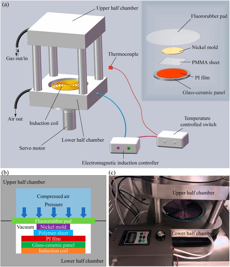
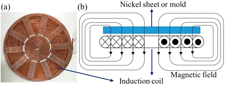
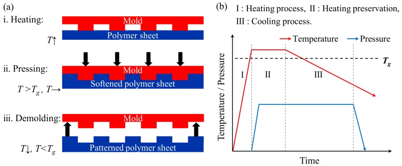
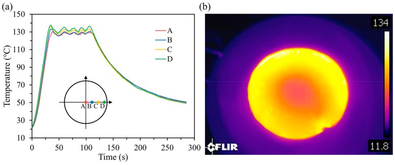
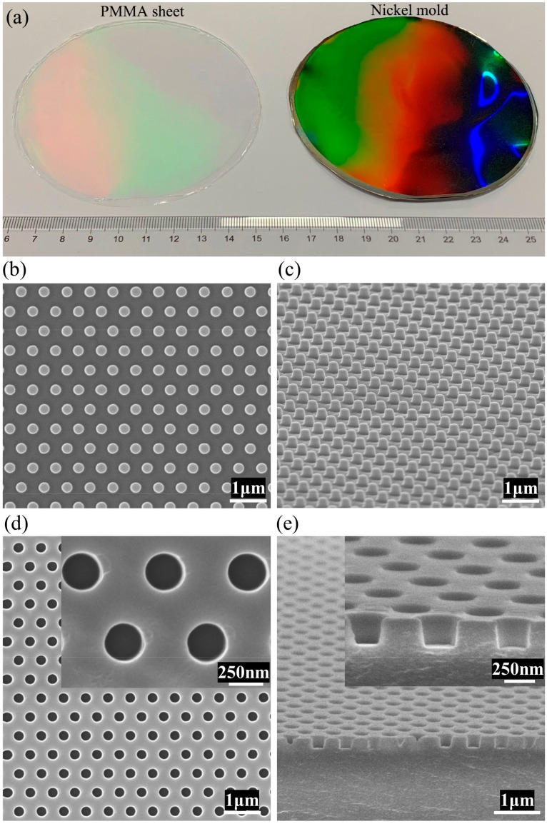
Thermal nanoimprint lithography is playing a vital role in fabricating micro/nanostructures on polymer materials by the advantages of low cost, high throughput, and high resolution. However, a typical thermal nanoimprint process usually takes tens of minutes due to the relatively low heating and cooling rate in the thermal imprint cycle. In this study, we developed an induction heating apparatus for the thermal imprint with a mold made of ferromagnetic material, nickel. By applying an external high-frequency alternating magnetic field, heat was generated by the eddy currents and magnetic hysteresis losses of the ferromagnetic nickel mold at high speed. Once the external alternating magnetic field was cut off, the system would cool down fast owe to the small thermal capacity of the nickel mold; thus, providing a high heating and cooling rate for the thermal nanoimprint process. In this paper, nanostructures were successfully replicated onto polymer sheets with the scale of 4-inch diameter within 5 min.
Overview
The claims and statistics of this paper haven’t been checked yet.
Run the check — free, no account needed. It reads the open-access text and checks the sources it cites.
Integrity signals
Registry
Cites
Statistics
Figures
Verification
Claims the paper makes
The claims and statistics of this paper haven’t been checked yet.
Run the check — free, no account needed. It reads the open-access text and checks the sources it cites.
Claims other papers make about this one
Each is checked against this paper’s own text: does it say what the citing paper says it does?
In the citing paper
“The technological parameters required variations in broad ranges in output power of 10-200 kW, inductor currents up to thousands of amps, low or high inductor voltages and resonant frequencies up to 300 kHz.”
Self-check
Percentages, sums and reported differences re-computed from the paper’s own numbers.
The self-check needs the paper’s full text.
Citations
Cites
No references could be resolved yet.
Research works printed but not linked: 59
- Moonen, 2012, Fabrication of transistors on flexible substrates: From mass-printing to high-resolution alternative lithography strategies, Adv. Mater., 24, 5526, 10.1002/adma.201202949 · DOI
- Zhao, 2011, The role of nanomaterials in redox-based supercapacitors for next generation energy storage devices, Nanoscale, 3, 839, 10.1039/c0nr00594k · DOI
- Li, 2000, Fabrication of circular optical structures with a 20 nm minimum feature size using nanoimprint lithography, Appl. Phys. Lett., 76, 673, 10.1063/1.125896 · DOI
- Shneidman, 2018, All-Polymer Integrated Optical Resonators by Roll-to-Roll Nanoimprint Lithography, Acs Photonics, 5, 1839, 10.1021/acsphotonics.8b00022 · DOI
- Khan, 2015, Technologies for Printing Sensors and Electronics Over Large Flexible Substrates: A Review, IEEE Sens. J., 15, 3164, 10.1109/JSEN.2014.2375203 · DOI · Paper page
- Kang, K., Cho, Y., and Yu, K.J. (2018). Novel Nano-Materials and Nano-Fabrication Techniques for Flexible Electronic Systems. Micromachines, 9. · DOI
- Chen, 2017, PVDF-Based Ferroelectric Polymers in Modern Flexible Electronics, Adv. Electron. Mater., 3, 1600460, 10.1002/aelm.201600460 · DOI
- Economou, 2018, Flexible plastic, paper and textile lab-on-a chip platforms for electrochemical biosensing, Lab Chip, 18, 1812, 10.1039/C8LC00025E · DOI
- Lee, 2015, Micropatterned P (VDF-TrFE) Film-Based Piezoelectric Nanogenerators for Highly Sensitive Self-Powered Pressure Sensors, Adv. Funct. Mater., 25, 3203, 10.1002/adfm.201500856 · DOI
- Peng, R. (2017). Towards Personal Health Monitoring: Detecting Biomolecules with Microfluidics and Nanoplasmonic Sensors Fabricated by Nanoimprint Lithography. [Ph.D. Thesis, Princeton University].
- Eom, 2015, Nanotextured Polymer Substrate for Flexible and Mechanically Robust Metal Electrodes by Nanoimprint Lithography, ACS Appl. Mater. Interfaces, 7, 25171, 10.1021/acsami.5b06631 · DOI
- Dascal, 2017, Virtual Reality and Medical Inpatients: A Systematic Review of Randomized, Controlled Trials, Innov. Clin. Neurosci., 14, 14
- Yew, 2016, Towards a griddable distributed manufacturing system with augmented reality interfaces, Rob. Comp. Integr. Manuf., 39, 43, 10.1016/j.rcim.2015.12.002 · DOI
- Wang, 2016, A comprehensive survey of augmented reality assembly research, Adv. Manuf., 4, 1, 10.1007/s40436-015-0131-4 · DOI
- Zhou, F., Duh, H.B.-L., and Billinghurst, M. Trends in augmented reality tracking, interaction and display: A review of ten years of ISMAR. Proceedings of the 7th IEEE/ACM International Symposium on Mixed and Augmented Reality.
- Park, 2008, Nanoscale patterning and electronics on flexible substrate by direct nanoimprinting of metallic nanoparticles, Adv. Mater., 20, 489, 10.1002/adma.200702326 · DOI
- Choi, 2015, One-Step Fabrication of Transparent and Flexible Nanotopographical-Triboelectric Nanogenerators via Thermal Nanoimprinting of Thermoplastic Fluoropolymers, Adv. Mater., 27, 7386, 10.1002/adma.201503802 · DOI
- Liang, 2015, Nanoimprinting of Flexible Polycarbonate Sheets with a Flexible Polymer Mold and Application to Superhydrophobic Surfaces, Adv. Mater. Interfaces, 2, 1500030, 10.1002/admi.201500030 · DOI
- Qiao, 2016, Toward Scalable Flexible Nanomanufacturing for Photonic Structures and Devices, Adv. Mater., 28, 10353, 10.1002/adma.201601801 · DOI
- Leitgeb, 2016, Multilength Scale Patterning of Functional Layers by Roll-to-Roll Ultraviolet-Light-Assisted Nanoimprint Lithography, ACS Nano, 10, 4926, 10.1021/acsnano.5b07411 · DOI
- Takei, 2015, Toward flexible and wearable human-interactive health-monitoring devices, Adv. Healthcare Mater., 4, 487, 10.1002/adhm.201400546 · DOI
- Sannicolo, 2016, Metallic nanowire-based transparent electrodes for next generation flexible devices: A Review, Small, 12, 6052, 10.1002/smll.201602581 · DOI
- Rajan, K., Garofalo, E., and Chiolerio, A. (2018). Wearable Intrinsically Soft, Stretchable, Flexible Devices for Memories and Computing. Sensors, 18. · DOI
- Guo, 2007, Nanoimprint lithography: Methods and material requirements, Adv. Mater., 19, 495, 10.1002/adma.200600882 · DOI
- Ahn, 2009, Large-area roll-to-roll and roll-to-plate nanoimprint lithography: A step toward high-throughput application of continuous nanoimprinting, ACS Nano, 3, 2304, 10.1021/nn9003633 · DOI
- Hirai, 2003, Defect analysis in thermal nanoimprint lithography, J. Vac. Sci. Technol. B, 21, 2765, 10.1116/1.1629289 · DOI
- Xia, 2003, Ultrafast patterning of nanostructures in polymers using laser assisted nanoimprint lithography, Appl. Phys. Lett., 83, 4417, 10.1063/1.1630162 · DOI
- Xia, 2010, Self-aligned memristor cross-point arrays fabricated with one nanoimprint lithography step, Nano Lett., 10, 2909, 10.1021/nl1017157 · DOI
- Austin, 2004, Fabrication of 5 nm linewidth and 14 nm pitch features by nanoimprint lithography, Appl. Phy. Lett., 84, 5299, 10.1063/1.1766071 · DOI
- Pourdavoud, 2017, Photonic nanostructures patterned by thermal nanoimprint directly into organo-metal halide perovskites, Adv. Mater., 29, 1605003, 10.1002/adma.201605003 · DOI
- Chou, 1995, Imprint of sub-25 nm vias and trenches in polymers, Appl. Phys. Lett., 67, 3114, 10.1063/1.114851 · DOI
- Chou, 1996, Imprint lithography with 25-nanometer resolution, Science, 272, 85, 10.1126/science.272.5258.85 · DOI
- Li, 2009, Hybrid nanoimprint-soft lithography with sub-15 nm resolution, Nano Lett., 9, 2306, 10.1021/nl9004892 · DOI
- Ge, 2005, Cross-linked polymer replica of a nanoimprint mold at 30 nm half-pitch, Nano Lett., 5, 179, 10.1021/nl048618k · DOI
- Li, 2006, Sub-20-nm alignment in nanoimprint lithography using Moire fringe, Nano Lett., 6, 2626, 10.1021/nl0603395 · DOI
- Ahn, 2008, High-speed roll-to-roll nanoimprint lithography on flexible plastic substrates, Adva. Mater., 20, 2044, 10.1002/adma.200702650 · DOI
- Schift, 2008, Nanoimprint lithography: An old story in modern times? A review, J. Vac. Sci. Technol. B, 26, 458, 10.1116/1.2890972 · DOI
- Fu, 2018, Top-down fabrication of shape-controlled, monodisperse nanoparticles for biomedical applications, Adv. Drug Deliv. Rev., 132, 169, 10.1016/j.addr.2018.07.006 · DOI
- Cui, 2015, Near-zero-residual layer nanoimprint based on hybrid nanoimprint soft lithography, Appl. Phys. A, 121, 371, 10.1007/s00339-015-9195-z · DOI
- Kimerling, 2006, Rapid hot embossing of polymer microfeatures, Microsyst. Technol., 12, 730, 10.1007/s00542-006-0098-y · DOI
- Chang, 2005, Development of fluid-based heating and pressing systems for micro hot embossing, Microsyst. Technol., 11, 396, 10.1007/s00542-004-0481-5 · DOI
- Lu, 2005, Analysis of laser/IR-assisted microembossing, Polym. Eng. Sci., 45, 661, 10.1002/pen.20324 · DOI
- Grewell, D., Lu, C., Lee, L.J., and Benatar, A. (2004). Infrared Micro-Embossing of Thermoplastics. ANTEC Conference Proceedings, John Wiley & Sons.
- Liu, 2005, Ultrasonic vibration hot embossing—A novel technique for molding plastic microstructure, Int. Polym. Process., 20, 449, 10.1515/ipp-2005-0074 · DOI
- Yao, 2002, Increasing flow length in thin wall injection molding using a rapidly heated mold, Polym. Plast. Technol. Eng., 41, 819, 10.1081/PPT-120014390 · DOI
- Yao, 2002, Development of rapid heating and cooling systems for injection molding applications, Polym. Eng. Sci., 42, 2471, 10.1002/pen.11133 · DOI
- Hong, S.-K., Heo, Y.-M., and Kang, J. (2008). Replication of Polymeric Micro Patterns by Rapid Thermal Pressing with Induction Heating Apparatus. 2008 3rd IEEE International Conference on Nano/Micro Engineered and Molecular Systems, IEEE. · DOI
- Guo, 2004, Recent progress in nanoimprint technology and its applications, J. Phys. D Appl. Phys., 37, R123, 10.1088/0022-3727/37/11/R01 · DOI
- Tormen, 2008, Fast thermal nanoimprint lithography by a stamp with integrated heater, Microelectron. Eng., 85, 1229, 10.1016/j.mee.2008.01.065 · DOI
- Kurose, 2009, 3-D Eddy Current Analysis of Induction Heating Apparatus Considering Heat Emission, Heat Conduction, and Temperature Dependence of Magnetic Characteristics, IEEE Trans. Magn., 45, 1847, 10.1109/TMAG.2009.2012829 · DOI
- Fagan, 2009, A novel process for continuous thermal embossing of large-area nanopatterns onto polymer films, Adv. Polym. Technol., 28, 246, 10.1002/adv.20167 · DOI
- Lucia, 2014, Induction Heating Technology and Its Applications: Past Developments, Current Technology, and Future Challenges, IEEE Trans. Ind. Electron., 61, 2509, 10.1109/TIE.2013.2281162 · DOI
- Rudnev, V., Loveless, D., and Cook, R.L. (2017). Handbook of Induction Heating, CRC Press. · DOI
- Cai, 2016, Induction-heated nanoimprint on soda-lime glass using sapphire molds, J. Vac. Sci. Technol. B, 34, 06K408, 10.1116/1.4966557 · DOI
- Huang, 2009, Experimental rapid surface heating by induction for micro-injection molding of light-guided plates, J. Appl. Polym. Sci., 113, 1345, 10.1002/app.30053 · DOI
- Chaboudez, 1997, Numerical modeling in induction heating for axisymmetric geometries, IEEE Trans. Magn., 33, 739, 10.1109/20.560107 · DOI
- Lee, 2016, High-resolution, high-aspect-ratio iridium–nickel composite nanoimprint molds, J. Vac. Sci. Technol. B, 34, 061804, 10.1116/1.4967696 · DOI
- Xie, 2017, Rapid fabrication of bio-inspired nanostructure with hydrophobicity and antireflectivity on polystyrene surface replicating from cicada wings, Nanoscale, 9, 11951, 10.1039/C7NR04176D · DOI
- Park, 2004, Anti-adhesive layers on nickel stamps for nanoimprint lithography, Microelectron. Eng., 73-4, 196, 10.1016/S0167-9317(04)00098-X · DOI
Cited by
Dimitrov, B., Hayatleh, K., Barker, S., & Collier, G. (2021) · Electricity · doi:10.3390/electricity2040026 · Cited by 3
Metadata
- Authors
- Fu, X., Chen, Q., Chen, X., Zhang, L., Yang, A., Cui, Y., Yuan, C., & Ge, H.
- Venue
- Micromachines
- Publisher
- MDPI AG
- Published
- 2019-05-21
- Volume
- 10
- Issue
- 5
- Pages
- 334
- ISSN
- 2072-666X
- PMC
- PMC6562963
- Cited by
- 17
- References
- 0
- Language
- en
- Funders
- National Key R&D Program of China (2018YFB1105400)
- National Natural Science Foundation of China (51721001)
About these checks
Registry, retraction, Cites and statistics results are computed, not judged, with one exception: a printed reference that no index lists is read once by a model before it counts as a citation error. Claims are extracted by a model and kept only when their quote appears verbatim in the text; each cited source is then checked, with a model’s help, for whether it says what the claim relies on. Those verdicts can be wrong — read the claim’s quote and the cited source before relying on one.
Statistics and arithmetic are recomputed, not judged.
Confidence bands are shown only for fields calibrated on our annotated test set. None is calibrated yet, so no band is shown.
What counts as a claim ›How we measure confidence ›How we check this ›
Are you an author, or do you see a problem with this page? Request a review
How to cite
Cite CoChat for the checks on this page, and the paper for its own findings.
- This page
- CoChat. (2026). Citation check: A Rapid Thermal Nanoimprint Apparatus through Induction Heating of Nickel Mold. https://app.cochat.ai/papers/10.3390/mi10050334
- The paper
- Fu, X., Chen, Q., Chen, X., Zhang, L., Yang, A., Cui, Y., Yuan, C., & Ge, H. (2019). A Rapid Thermal Nanoimprint Apparatus through Induction Heating of Nickel Mold. Micromachines. https://doi.org/10.3390/mi10050334
Data sources
Bibliographic data: Semantic Scholar, OpenAlex, Crossref.
Contains information from the Semantic Scholar Academic Graph Datasets, made available under the ODC Attribution License (ODC-BY 1.0).
Semantic Scholar’s data is described in: Kinney, R., et al. (2023). The Semantic Scholar Open Data Platform. arXiv:2301.10140.
