

In‐Memory Vector‐Matrix Multiplication in Monolithic Complementary Metal–Oxide–Semiconductor‐Memristor Integrated Circuits: Design Choices, Challenges, and Perspectives
Open accessThe DOI matches its Crossref record; 93 of the 93 references it cites were found in a registry or an index.
Abstract
The low communication bandwidth between memory and processing units in conventional von Neumann machines does not support the requirements of emerging applications that rely extensively on large sets of data. More recent computing paradigms, such as high parallelization and near‐memory computing, help alleviate the data communication bottleneck to some extent, but paradigm‐shifting concepts are required. In‐memory computing has emerged as a prime candidate to eliminate this bottleneck by colocating memory and processing. In this context, resistive switching (RS) memory devices is a key promising choice, due to their unique intrinsic device‐level properties, enabling both storing and computing with a small, massively‐parallel footprint at low power. Theoretically, this directly translates to a major boost in energy efficiency and computational throughput, but various practical challenges remain. A qualitative and quantitative analysis of several key existing challenges in implementing high‐capacity, high‐volume RS memories for accelerating the most computationally demanding computation in machine learning (ML) inference, that of vector‐matrix multiplication (VMM), is presented. The monolithic integration of RS memories with complementary metal–oxide–semiconductor (CMOS) integrated circuits is presented as the core underlying technology. The key existing design choices in terms of device‐level physical implementation, circuit‐level design, and system‐level considerations is reviewed and an outlook for future directions is provided.
Overview
The claims and statistics of this paper haven’t been checked yet.
Free: it reads the open-access text and checks the first 5 claims that cite a source we can check. Create a free account to check every claim.
Integrity signals
Registry
Cites
Statistics
Figures
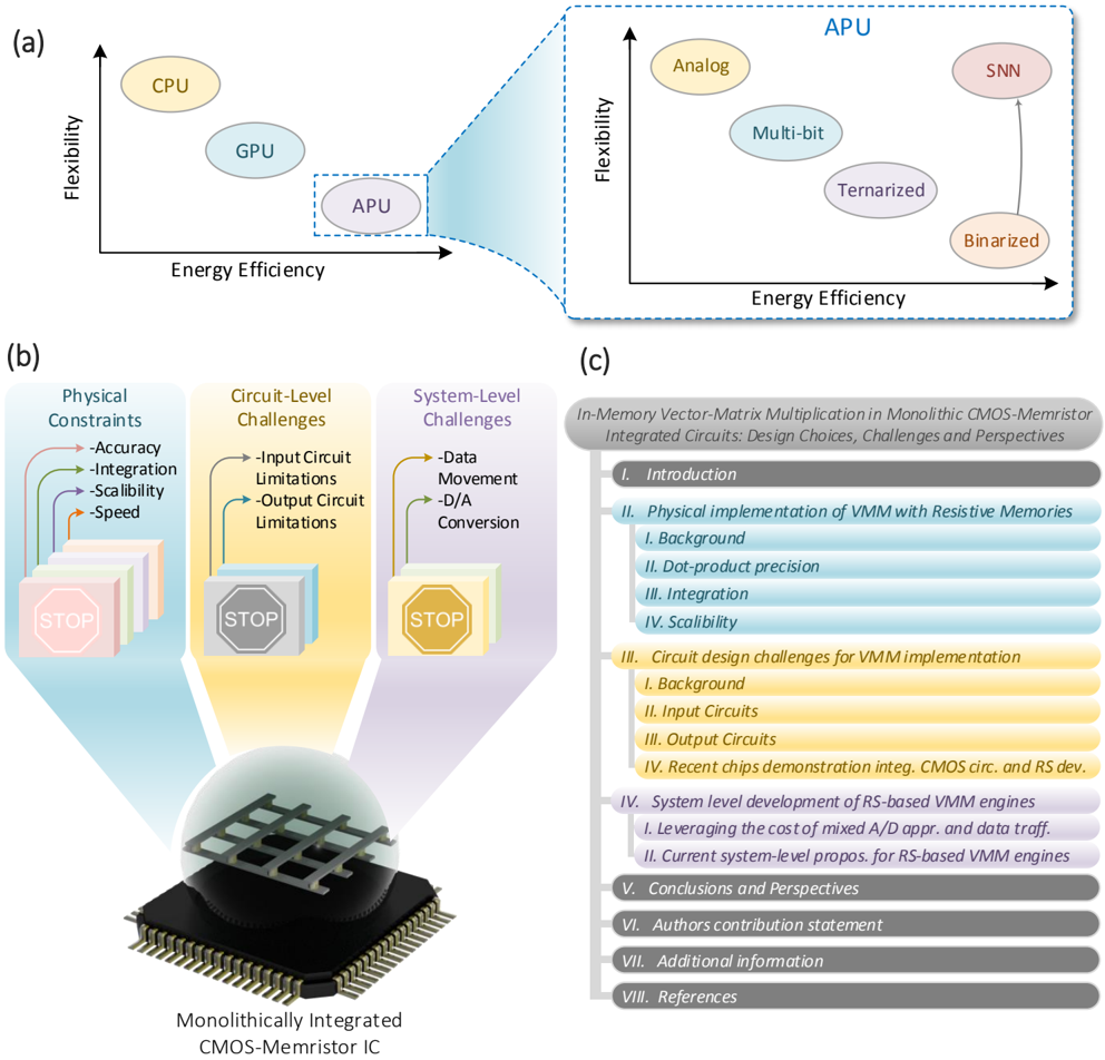
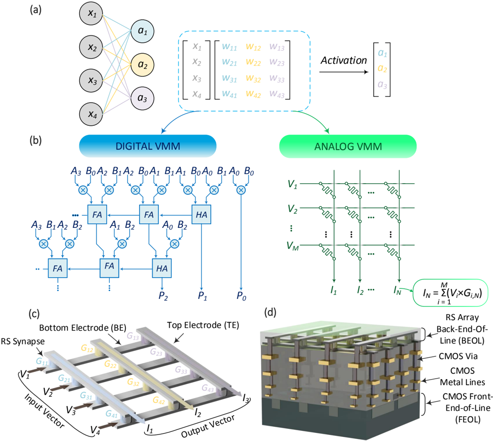
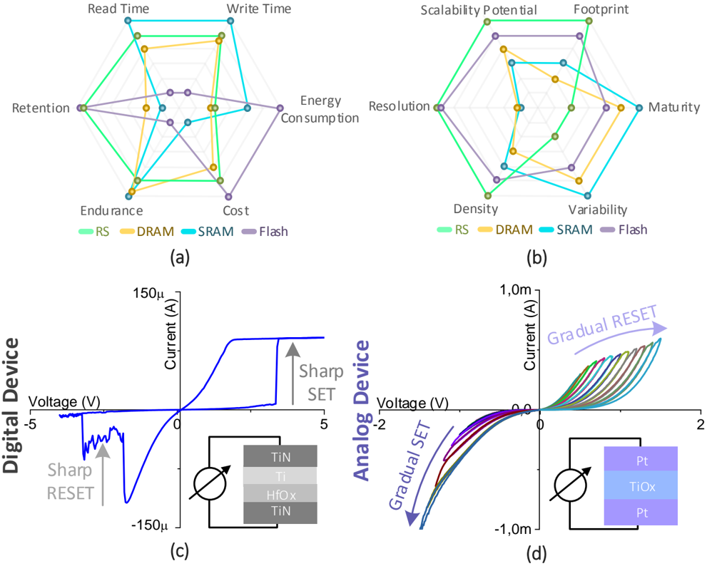
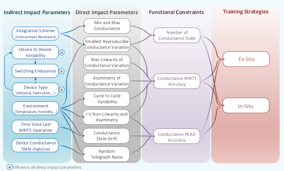

Verification
Claims the paper makes
The claims and statistics of this paper haven’t been checked yet.
Free: it reads the open-access text and checks the first 5 claims that cite a source we can check. Create a free account to check every claim.
Claims other papers make about this one
Each is checked against this paper’s own text: does it say what the citing paper says it does?
The source backs part of the claim, not all of it — or backs it for a different population, condition or comparison.
In the citing paper
“Although very popular102,113–116, this approach might be limited for the case of the smallest technology nodes implementations as the gain and bandwidth of the amplifiers are limited by the intrinsic transistor gain95,117.”
From Hardware implementation of memristor-based artificial neural networks (2024) · cites this paper as [95]
Experimental — accuracy not yet measuredThe source backs part of the claim, not all of it — or backs it for a different population, condition or comparison.
In the citing paper
“SAR-ADC and controlled oscillator-based ADCs (Current-Controlled-Oscillators -CCO, see Fig. 11c- and Voltage-Controlled-Oscillators -VCO, Fig. 11d-) are more suitable to smaller technology node implementations95,117.”
From Hardware implementation of memristor-based artificial neural networks (2024) · cites this paper as [95]
Experimental — accuracy not yet measuredThe source backs part of the claim, not all of it — or backs it for a different population, condition or comparison.
In the citing paper
“A cost-effective recurrent solution has been to use a smaller number of DACs and share them among different rows by adding a layer of analogue multiplexors between the DACs and the wordline inputs93,95,221. With this approach (which we could refer to as On-chip time-multiplexed analogue input – Analogue/Multilevel weights), a given VMM operation is divided in n different sub-VMM operations and the”
From Hardware implementation of memristor-based artificial neural networks (2024) · cites this paper as [95]
Experimental — accuracy not yet measuredThe cited source says what the claim attributes to it.
In the citing paper
“For DAC relying in resistors, the major noise source is from the CMOS operational amplifier in the output stage95, and it can be minimized using larger transistors (both in width and length) for the differential input pair.”
From Hardware implementation of memristor-based artificial neural networks (2024) · cites this paper as [95]
Self-check
Percentages, sums and reported differences re-computed from the paper’s own numbers.
The self-check needs the paper’s full text.
Citations
Cites
LeCun, Y., Bengio, Y., & Hinton, G. (2015) · Nature · doi:10.1038/nature14539 · Cited by 84,126
Strukov, D. B., Snider, G. S., Stewart, D. R., & Williams, R. S. (2008) · Nature · doi:10.1038/nature06932 · Cited by 11,828
Memristor—The Missing Circuit Element
Chua, L. (1971) · IEEE Transactions on Circuit Theory · doi:10.1109/tct.1971.1083337 · Cited by 10,268
In situ click chemistry generation of cyclooxygenase-2 inhibitors
Bhardwaj, A., Kaur, J., Wuest, M., & Wuest, F. (2017) · Nature Communications · doi:10.1038/s41467-016-0009-6 · Cited by 7,448
Structural absorption by barbule microstructures of super black bird of paradise feathers
McCoy, D. E., Feo, T., Harvey, T. A., & Prum, R. O. (2018) · Nature Communications · doi:10.1038/s41467-017-02088-w · Cited by 7,424
Cramming More Components Onto Integrated Circuits
Moore, G. E. (1998) · Proceedings of the IEEE · doi:10.1109/jproc.1998.658762 · Cited by 5,926
In-Datacenter Performance Analysis of a Tensor Processing Unit
Jouppi, N. P., Young, C., Patil, N., Patterson, D., Agrawal, G., Bajwa, R., Bates, S., Bhatia, S., Boden, N., Borchers, A., et al. (2017) · Proceedings of the 44th Annual International Symposium on Computer Architecture · doi:10.1145/3079856.3080246 · Cited by 4,537
Eyeriss: An Energy-Efficient Reconfigurable Accelerator for Deep Convolutional Neural Networks
Chen, Y.-H., Krishna, T., Emer, J. S., & Sze, V. (2017) · IEEE Journal of Solid-State Circuits · doi:10.1109/jssc.2016.2616357 · Cited by 3,247
Analog Integrated Circuit Design
Carusone, A. C., Johns, D. A., & Martin, K. W. (1996) · Cited by 2,509
In-memory computing with resistive switching devices
Ielmini, D., & Wong, H.-S. P. (2018) · Nature Electronics · doi:10.1038/s41928-018-0092-2 · Cited by 2,298
Research works printed but not linked: 41
- 2. Horowitz, M. 1.1 computing's energy problem (and what we can do about it). In 2014 IEEE International Solid-State Circuits Conference Digest of Technical Papers (ISSCC) , 10-14 (IEEE, 2014).
- 8. Sze, V., Chen, Y.-H., Emer, J., Suleiman, A. & Zhang, Z. Hardware for machine learning: Challenges and opportunities. In 2017 IEEE Custom Integrated Circuits Conference (CICC) , 1-8 (IEEE, 2017). · DOI · Paper page
- 16. Bojnordi, M. N. & Ipek, E. Memristive boltzmann machine: A hardware accelerator for combinatorial optimization and deep learning. In 2016 IEEE International Symposium on High Performance Computer Architecture (HPCA) , 1-13 (IEEE, 2016). · DOI · Paper page
- 19. Shin, J. H., Jeong, Y. J., Zidan, M. A., Wang, Q. & Lu, W. D. Hardware acceleration of simulated annealing of spin glass by rram crossbar array. In 2018 IEEE International Electron Devices Meeting (IEDM) , 3-3 (IEEE, 2018). · DOI · Paper page
- 25. Wu, T. F. et al. Brain-inspired computing exploiting carbon nanotube fets and resistive ram: Hyperdimensional computing case study. In 2018 IEEE International Solid-State Circuits Conference-(ISSCC) , 492-494 (IEEE, 2018).
- 28. Song, L., Qian, X., Li, H. & Chen, Y. Pipelayer: A pipelined reram-based accelerator for deep learning. In 2017 IEEE International Symposium on High Performance Computer Architecture (HPCA) , 541-552 (IEEE, 2017). · DOI · Paper page
- 29. Sebastian, A. et al. Computational memory-based inference and training of deep neural networks. In 2019 Symposium on VLSI Technology , T168-T169 (IEEE, 2019). · DOI
- 31. Mahmoodi, M. et al. Ultra-low power physical unclonable function with nonlinear fixed-resistance crossbar circuits. In 2019 IEEE International Electron Devices Meeting (IEDM) , 30-1 (IEEE, 2019). · doi:10.1109/iedm19573.2019.8993618
- 38. Yan, B. et al. Rram-based spiking nonvolatile computing-in-memory processing engine with precisionconfigurable in situ nonlinear activation. In 2019 Symposium on VLSI Technology , T86-T87 (IEEE, 2019). · DOI · Paper page
- 40. Gupta, I. et al. Real-time encoding and compression of neuronal spikes by metal-oxide memristors. Nat. communications 7 , 1-9 (2016).
- 59. Govoreanu, B. et al. 10 × 10nm 2 hf/hfo x crossbar resistive ram with excellent performance, reliability and low-energy operation. In 2011 International Electron Devices Meeting , 31-6 (IEEE, 2011).
- 48. Wu, T. F. et al. 14.3 a 43pj/cycle non-volatile microcontroller with 4.7 m s shutdown/wake-up integrating 2.3-bit/cell resistive ram and resilience techniques. In 2019 IEEE International Solid-State Circuits Conference(ISSCC) , 226-228 (IEEE, 2019).
- B.Govoreanu G.Kar Y.Chen V.Paraschiv S.Kubicek A.Fantini I.Radu L.Goux S.Clima R.Degraeve N.Jossart O.Richard T.Vandeweyer K.Seo P.Hendrickx G.Pourtois H.Bender L.Altimime D. J.Wouters J. A.Kittl M.Jurczak in2011 Int. Electron Devices Meeting IEEE Piscataway NJ2011 pp.31–36. · DOI · Paper page
- 68. Fantini, A. et al. Intrinsic switching variability in hfo 2 rram. In 2013 5th IEEE International Memory Workshop , 30-33 (IEEE, 2013). · DOI · Paper page
- 71. Chen, P.-Y. et al. Mitigating effects of non-ideal synaptic device characteristics for on-chip learning. In 2015 IEEE/ACM International Conference on Computer-Aided Design (ICCAD) , 194-199 (IEEE, 2015).
- 73. Fantini, A. et al. Intrinsic program instability in hfo2 rram and consequences on program algorithms. In 2015 IEEE International Electron Devices Meeting (IEDM) , 7.5.1-7.5.4 (2015). · DOI
- 74. Lee, H. et al. Evidence and solution of over-reset problem for hfo x based resistive memory with sub-ns switching speed and high endurance. In 2010 International Electron Devices Meeting , 19-7 (IEEE, 2010). · DOI · Paper page
- 82. Murmann, B. ADC Performance Survey 1997-2020 (2020).
- 87. Hashemi, S., Anthony, N., Tann, H., Bahar, R. I. & Reda, S. Understanding the impact of precision quantization on the accuracy and energy of neural networks. In Design, Automation & Test in Europe Conference & Exhibition (DATE), 2017 , 1474-1479 (IEEE, 2017).
- 89. Su, F. et al. A 462gops/j rram-based nonvolatile intelligent processor for energy harvesting ioe system featuring nonvolatile logics and processing-in-memory. In 2017 Symposium on VLSI Technology , T260-T261 (IEEE, 2017).
- 90. Bocquet, M. et al. In-memory and error-immune differential rram implementation of binarized deep neural networks. In 2018 IEEE International Electron Devices Meeting (IEDM) , 20-6 (IEEE, 2018). · DOI · Paper page
- 92. Liu, Q. et al. 33.2 a fully integrated analog reram based 78.4 tops/w compute-in-memory chip with fully parallel mac computing. In 2020 IEEE International Solid-State Circuits Conference-(ISSCC) , 500-502 (IEEE, 2020).
- 93. Mochida, R. et al. A 4m synapses integrated analog reram based 66.5 tops/w neural-network processor with cell current controlled writing and flexible network architecture. In 2018 IEEE Symposium on VLSI Technology , 175-176 (IEEE, 2018).
- 94. Xue, C.-X. et al. 24.1 a 1mb multibit reram computing-in-memory macro with 14.6 ns parallel mac computing time for cnn based ai edge processors. In 2019 IEEE International Solid-State Circuits Conference-(ISSCC) , 388-390 (IEEE, 2019).
- Q.Liu B.Gao P.Yao D.Wu J.Chen Y.Pang W.Zhang Y.Liao C.-X.Xue W.-H.Chen J.Tang Y.Wang M.-F.Chang H.Qian H.Wu in2020 IEEE Int. Solid-State Circuits Conf.-(ISSCC) IEEE Piscataway NJ2020 pp.500–502.
- 99. Karatsuba, A. A. & Ofman, Y. P. Multiplication of many-digital numbers by automatic computers. In Doklady Akademii Nauk , vol. 145, 293-294 (Russian Academy of Sciences, 1962).
- 100. Huss-Lederman, S., Jacobson, E. M., Johnson, J. R., Tsao, A. & Turnbull, T. Strassen's algorithm for matrix multiplication: Modeling, analysis, and implementation. In Proceedings of Supercomputing , vol. 96, 9-6 (Citeseer, 1996).
- 103. Bavandpour, M., Mahmoodi, M. R. & Strukov, D. acortex: An energy-efficient multi-purpose mixed-signal inference accelerator. accepted, IEEE J. Explor. Solid-State Comput. Devices Circuits (2020).
- 104. Bavandpour, M., Sahay, S., Mahmoodi, M. R. & Strukov, D. Efficient mixed-signal neurocomputing via successive integration and rescaling. IEEE Transactions on Very Large Scale Integration (VLSI) Syst. (2019).
- 108. Moons, B., Uytterhoeven, R., Dehaene, W. & Verhelst, M. 14.5 envision: A 0.26-to-10tops/w subword-parallel dynamic-voltage-accuracy-frequency-scalable convolutional neural network processor in 28nm fdsoi. In 2017 IEEE International Solid-State Circuits Conference (ISSCC) , 246-247 (IEEE, 2017).
- 109. Merritt, R. Startup Accelerates AI at the Sensor (2019).
- 110. Shin, D., Lee, J., Lee, J. & Yoo, H.-J. 14.2 dnpu: An 8.1 tops/w reconfigurable cnn-rnn processor for general-purpose deep neural networks. In 2017 IEEE International Solid-State Circuits Conference (ISSCC) , 240-241 (IEEE, 2017).
- 115. Google. Edge TPU: Google's purpose-built ASIC designed to run inference at the edge (2019).
- 117. Cutress, I. Cambricon, maker of hauwei's kirin npu ip, build a big ai chip and pcie card (2018).
- 118. Armasu, L. Move Over GPUs: Startup's Chip Claims to Do Deep Learning Inference Better (2018).
- 119. Ueyoshi, K. et al. Quest: A 7.49 tops multi-purpose log-quantized dnn inference engine stacked on 96mb 3d sram using inductive-coupling technology in 40nm cmos. In 2018 IEEE International Solid-State Circuits Conference-(ISSCC) , 216-218 (IEEE, 2018).
- 121. Hruska, J. New Movidius Myriad X VPU Packs a Custom Neural Compute Engine (2017).
- 124. Chen, Y. et al. Dadiannao: A machine-learning supercomputer. In 2014 47th Annual IEEE/ACM International Symposium on Microarchitecture , 609-622 (IEEE, 2014). · DOI · Paper page
- 125. Rockchip. Rockchip Released Its First AI Processor RK3399Pro NPU Performance up to 2.4TOPs (2018).
- R.Mochida K.Kouno Y.Hayata M.Nakayama T.Ono H.Suwa R.Yasuhara K.Katayama T.Mikawa Y.Gohou in2018 IEEE Symp. on VLSI Technology IEEE Piscataway NJ2018 pp.175–176. · DOI · Paper page
- C.-X.Xue W.-H.Chen J.-S.Liu J.-F.Li W.-Y.Lin W.-E.Lin J.-H.Wang W.-C.Wei T.-W.Chang T.-C.Chang T.-Y.Huang H.-Y.Kao S.-Y.Wei Y.-C.Chiu C.-Y.Lee C.-C.Lo Y.-C.King C.-J.Lin R.-S.Liu C.-C.Hsieh K.-T.Tang M.-F.Chang in2019 IEEE Int. Solid-State Circuits Conf.-(ISSCC) IEEE Piscataway NJ2019 pp.388–390.
Cited by
Items 101–200 of 216
Electrical Characteristics of CMOS-Compatible SiOx-Based Resistive-Switching Devices
Koryazhkina, M. N., Filatov, D. O., Tikhov, S. V., Belov, A. I., Serov, D. A., Kryukov, R. N., Zubkov, S. Y., Vorontsov, V. A., Павлов, Д. А., Gryaznov, E. G., et al. (2023) · Nanomaterials · doi:10.3390/nano13142082 · Cited by 5
“In addition, a simple structure of the memristive device stack allows for the development of super-dense and potentially three-dimensional cross-bar arrays, which implement the vector–matrix multiplication operations underlying inference in traditional deep learning artificial neural networks [5,6] and new learning al…”
BackgroundJiménez-Molinos, F., Vinuesa, G., García, H., Dueñas, S., Castán, H., González, M. B., Campabadal, F., & Roldán, J. B. (2024) · Materials Science in Semiconductor Processing · doi:10.1016/j.mssp.2024.108480 · Cited by 6
Dong, X., Chen, B., Genov, R., Azghadi, M. R., & Amirsoleimani, A. (2024) · Neurocomputing · doi:10.1016/j.neucom.2024.128275 · Cited by 5
Self-citationCluster-type conductive path-based selector-less 1R memristor array for spiking neural networks
Kim, J. E., Hu, S., Kwon, J. Y., Chun, S. Y., Soh, K., Yun, H., Baek, S., Nahm, S., Jeong, Y. J., & Yoon, J. H. (2025) · Nano Energy · doi:10.1016/j.nanoen.2025.110983 · Cited by 5
Myoung, S. J., Shin, D. H., Cho, J. R., Kim, S., Jeon, S. H., Kim, W., Lee, J., Kim, C., Bae, J., Choi, S., et al. (2025) · Materials Science in Semiconductor Processing · doi:10.1016/j.mssp.2025.109897 · Cited by 5
Memristive floating-point Fourier neural operator network for efficient scientific modeling
Li, J., Tian, J., Lin, Y., Zhou, Z., Li, Y., Gao, B., Tang, J., Chen, J., He, Y., Qian, H., et al. (2025) · Science Advances · doi:10.1126/sciadv.adv4446 · Cited by 5
Simulation of Calculation Errors in Memristive Crossbars for Artificial Neural Networks
Алексеевич, Б. И., Antonov, A., & Korolev, L. (2023) · International Conference on Industrial Engineering, Applications and Manufacturing (ICIEAM) · doi:10.1109/icieam57311.2023.10139308 · Cited by 4
“In ANNs, they are used to perform the operation of matrix-vector multiplication (MVM), which occurs in accordance with the natural physical Ohm's law [8].”
MethodPathways for electron device research in the AI era
Trommer, J. (2025) · Device · doi:10.1016/j.device.2024.100656 · Cited by 4
Mitigating State-Drift in Memristor Crossbar Arrays for Vector Matrix Multiplication
Amirsoleimani, A., Liu, T., Alibart, F., Eccofey, S., Chang, Y., Drouin, D., & Genov, R. (2021) · IntechOpen eBooks · doi:10.5772/intechopen.100246 · Cited by 6
Self-citationPossibilities and Limitations of Memristor Crossbars for Neuromorphic Computing
Telminov, O. A., & Gornev, E. (2022) · Scientific School Dynamics of Complex Networks and their Applications (DCNA) · doi:10.1109/dcna56428.2022.9923302 · Cited by 4
“The monolithic integration of ReRAM with CMOS is the core underlying technology nowadays [11].”
MethodPRUNIX: Non-Ideality Aware Convolutional Neural Network Pruning for Memristive Accelerators
Al-Shaarawy, A., Amirsoleimani, A., & Genov, R. (2022) · IEEE International Symposium on Circuits and Systems proceedings · doi:10.1109/iscas48785.2022.9937541 · Cited by 4
“This feature, when coupled with a crossbar architecture, affords us the computation of vector-matrix multiplication in the analog domain [10], since VMM is the backbone of neural network computation, one can easily see where the interest in this technology by the deep learning community arose from.”
BackgroundSelf-citationA Multichiplet Computing-in-Memory Architecture Exploration Framework Based on Various CIM Devices
Dai, Z., Xiang, F., Fu, X., He, Y., Sun, W., Liu, Y., Yang, G., Zhang, F., Yue, J., & Li, L. (2024) · IEEE Transactions on Computer-Aided Design of Integrated Circuits and Systems · doi:10.1109/tcad.2024.3416256 · Cited by 6
“By eliminating the heavy memory access and utilizing the high-internal computation parallelism, the computing-in-memory (CIM) architecture is a promising solution [1] to achieve higher-energy efficiency and higher performance [2] compared to the conventional von Neumann architecture.”
Heterogeneous density-based clustering with a dual-functional memristive array
Shin, D. H., Cheong, S., Lee, S. H., Jang, Y. H., Park, T., Han, J., Shim, S. K., Kim, Y. R., Han, J., Baek, I. K., et al. (2024) · Materials Horizons · doi:10.1039/d4mh00300d · Cited by 5
SDEX: Monte Carlo Simulation of Stochastic Differential Equations on Memristor Crossbars
Primeau, L., Amirsoleimani, A., & Genov, R. (2022) · IEEE International Symposium on Circuits and Systems proceedings · doi:10.1109/iscas48785.2022.9937861 · Cited by 4
“Despite their promise as VMM accelerators, current devices suffer from nonidealities stemming from immature fabrication techniques [1], preventing perfectly accurate VMM operations.”
BackgroundSelf-citationLambertini, A., Zanotti, T., Pavan, P., Padovani, A., & Puglisi, F. M. (2025) · APL Machine Learning · doi:10.1063/5.0274233 · Cited by 3
QuickNN: Python Toolbox for Training and Optimizing ANN for Hardware Implementation
Humood, K., Serb, A., Wang, S., & Prodromakis, T. (2023) · IEEE International Midwest Symposium on Circuits and Systems (MWSCAS) · doi:10.1109/mwscas57524.2023.10405963 · Cited by 3
“None of the above libraries allow binary/ternary quantization of the weights that are used in most state-of-the-art ANN designs [10].”
BackgroundMethodSustainable vertically-oriented graphene-electrode memristors for neuromorphic applications
Walters, B., Kamel, M. S. A., Jacob, M. V., & Azghadi, M. R. (2024) · FlatChem · doi:10.1016/j.flatc.2024.100755 · Cited by 3
“Memristors have many potential applications in both neuromorphic and other research, such as memristor-based neuromorphic chips [8], hardware security [9], vector – matrix multiplication [10] and various forms of neural networks [1].”
Robust quantum dots charge autotuning using neural network uncertainty
Yon, V., Galaup, B., Rohrbacher, C., Rivard, J., Godfrin, C., Li, R., Kubicek, S., Greve, K. D., Gaudreau, L., Dupont-Ferrier, E., et al. (2024) · Machine Learning Science and Technology · doi:10.1088/2632-2153/ad88d5 · Cited by 8
“This specialized hardware takes advantage of in-memory computing [86, 87] to efficiently perform the multiply–accumulate operations [88] required for NN inference.”
Self-citationGiacomo, S. D., Ronchi, M., Amadori, M., Borghi, G., Carminati, M., & Fiorini, C. E. (2025) · IEEE Transactions on Radiation and Plasma Medical Sciences · doi:10.1109/trpms.2025.3530774 · Cited by 4
“The appropriate selection will depend on the constraints and requirements of the application in question [54].”
SPIKA: 200-TOPS/W RRAM-based Neural Network Accelerator Chip
Humood, K., Foster, P., Wang, S., Serb, A., & Prodromakis, T. (2025) · IEEE International Symposium on Circuits and Systems proceedings · doi:10.1109/iscas56072.2025.11044289 · Cited by 3
“…Programme Grant EP/R024642/2 ”Functional Oxide Reconfigurable Technologies (FORTE)” and the RAEng Chair in Emerging Technologies (CiET1819/2/93). costs associated with input encoding, while also effectively mitigating the impact of RRAM devices’ inherent I-V non-linearity on output accuracy [3].”
Energy-efficient neural network design using memristive MAC unit
Yu, S., Bunnam, T., Triamlumlerd, S., Pracha, M., Xia, F., Shafik, R., & Yakovlev, A. (2022) · Frontiers in Electronics · doi:10.3389/felec.2022.877629 · Cited by 3
Maldonado, D., Belov, A. I., Koryazhkina, M. N., Jiménez-Molinos, F., Mikhaylov, A. N., & Roldán, J. B. (2022) · physica status solidi (a) · doi:10.1002/pssa.202200520 · Cited by 6
Artificially-Intelligent Fascicle-Selective Bidirectional Peripheral Nerve Interfaces
Xu, J., Filho, J. D. S., Hwang, E., Nag, S., Long, L., Kanchwala, M., Abdolrazzaghi, M., Huang, Y. T., Zariffa, J., & Genov, R. (2023) · IEEE Biomedical Circuits and Systems Conference (BioCAS) · doi:10.1109/biocas58349.2023.10388693 · Cited by 3
Self-citationChowdhury, M. T. R., Vo, H. Q. N., Ramanan, P., Yildirim, M., & Tütüncüoğlu, G. (2024) · International Conference on Neuromorphic Systems (ICONS) · doi:10.1109/icons62911.2024.00058 · Cited by 6
“…of the input voltages and the corresponding conductance values of each row, expressed mathematically as This mechanism underscores the computational efficiency inherent in the RRAM crossbar design for implementing VMM operations, with improved energy efficiency and reduced latency metrics [8–16].”
BackgroundIn-Memory Computation Using CMOS-Integrated Resistive RAM for Robotic Navigation
Solanki, J., Pelton, J., Febbo, R., Liehr, M., DeCandia, A., Beckmann, K., Rose, G. S., & Cady, N. C. (2024) · International Conference on Neuromorphic Systems (ICONS) · doi:10.1109/icons62911.2024.00038 · Cited by 3
“Voltage inputs (V1 to V8), as depicted in Fig 1, are then applied to the rows of the crossbar to carry out analog VMM, and the resulting currents in the columns (I out ) are measured [17].”
Digital Forensic on Secure Digital High Capacity using DFRWS Method
Yudhana, A., Riadi, I., & Putra, B. (2022) · Jurnal RESTI (Rekayasa Sistem dan Teknologi Informasi) · doi:10.29207/resti.v6i6.4615 · Cited by 3
“SDHC storage cards are hardware with an architecture that has similarities with other types of memory cards, namely monolithic[3]; SDHC is a further development of Secure Digital (SD) card storage hardware which can only accommodate up to a capacity of 2 gigabytes, in contrast to the largest SD card capacity.”
BackgroundA memristive neural decoder for cryogenic fault-tolerant quantum error correction
Yon, V., Marcotte, F., Mouny, P.-A., Dagnew, G. A., Kulchytskyy, B., Rochette, S., Beilliard, Y., Drouin, D., & Ronagh, P. (2025) · Quantum Science and Technology · doi:10.1088/2058-9565/adc3ba · Cited by 11
Self-citationDahiya, A., Kumar, S., & Rani, S. (2025) · IEEE Transactions on Electron Devices · doi:10.1109/ted.2025.3635115 · Cited by 3
“On the other hand, variability in the memristive device was a major obstacle to the wider acceptance of this memory technology [16].”
Fast prototyping of memristors for ReRAMs and neuromorphic computing
Marraccini, G., Strangio, S., Dimaggio, E., Sargeni, R., Pieri, F., Sozen, Y., Castellanos-Gómez, A., & Fiori, G. (2025) · Nanoscale · doi:10.1039/d5nr02690c · Cited by 3
Probing Traps in Ta 2 O 5 /Al 2 O 3 Memristive Switching Devices
Ranjan, A., Padovani, A., Torraca, P. L., Pan, J., Wang, W., Song, W., Bosman, M., Pey, K. L., & Raghavan, N. (2025) · ACS Applied Electronic Materials · doi:10.1021/acsaelm.5c01880 · Cited by 1
Multiplier-Free In-Memory Vector-Matrix Multiplication Using Distributed Arithmetic
Zeller, F., Reuben, J., & Fey, D. (2025) · IEEE International Symposium on Embedded Multicore/Many-core Systems-on-Chip (MCSoC) · doi:10.1109/mcsoc67473.2025.00116 · Cited by 2
“Vector Matrix Multiplication (VMM) is the fundamental and frequently required operation in neural networks, image processing, combinatorial optimization, solving linear equations, sparse coding, associative memories, reservoir computing and many signal processing applications [3], [4].”
Slipko, V. A., Ascoli, A., Corinto, F., & Pershin, Y. V. (2026) · Journal of Physics D Applied Physics · doi:10.1088/1361-6463/ae3f42 · Cited by 2
Mechanism and Evaluation of Two-Terminal Ferroelectric-Based Memristive/Memcapacitive Devices
Ahn, H. J., Shin, H. J., Yu, N. K., & Yoon, J. H. (2026) · Electronic Materials Letters · doi:10.1007/s13391-026-00634-7 · Cited by 3
“When assembled into crossbar arrays, these ferroelectric two-terminal devices can implement in-memory vector-matrix multiplication (VMM) based on Ohm’s and Kirch-hoff’s law ( I = G · V ), which is a core computational primitive in neuromorphic architectures [25, 26].”
Go, J. S., & Kim, J. T. (2026) · Electronics · doi:10.3390/electronics15061217 · Cited by 2
Tolerating Stuck-at Fault and Variation in Resistive Edge Inference Engine via Weight Mapping
Ma, Y., Zheng, L., & Zhou, P. (2021) · ACM Great Lakes Symposium on VLSI (GLSVLSI) · doi:10.1145/3453688.3461487 · Cited by 3
“Although the crossbar size can be large ideally, the size is always limited in reality [14] because of power and reliability issues [15].”
BackgroundSakhuja, J., Saraswat, V., Lashkare, S., & Ganguly, U. (2023) · IEEE Electron Devices Technology & Manufacturing Conference (EDTM) · doi:10.1109/edtm55494.2023.10103016 · Cited by 2
“Particularly, the analog computing capability of memristor devices greatly enhances modern computing systems' efficiency [2].”
BackgroundIn-Memory Transformer Self-Attention Mechanism Using Passive Memristor Crossbar
Cai, J., Kaleem, M. A., Genov, R., Azghadi, M. R., & Amirsoleimani, A. (2024) · IEEE International Symposium on Circuits and Systems proceedings · doi:10.1109/iscas58744.2024.10558182 · Cited by 3
“With its non-volatile nature and multi-bit capacity, memristors can perform efficient, low-footprint analog vector-matrix multiplication (VMM) in O( 1 ) when arranged in a crossbar [5]–[7].”
BackgroundSelf-citationSAR-MemPipe: A Hybrid Pipeline-SAR Memristive ADC for Analog Resistive Arrays
You, H., Xu, J., Amirsoleimani, A., Azghadi, M. R., & Genov, R. (2024) · IEEE International Symposium on Circuits and Systems proceedings · doi:10.1109/iscas58744.2024.10557966 · Cited by 3
“While vector-matrix multiplication (VMM) has taken most parts of neural network computing, in-memory computing with resistive crossbar architecture is developed to facilitate the efficiency of multiply and accumulate (MAC) operation in VMM [1]–[3].”
BackgroundSelf-citationSakhuja, J., Lashkare, S., & Ganguly, U. (2024) · Conference digest · doi:10.1109/drc61706.2024.10605467 · Cited by 2
Park, J.-H., Kim, S., & Choi, W. Y. (2024) · Advanced Intelligent Systems · doi:10.1002/aisy.202400673 · Cited by 2
Energy- and Area-Efficient CMOS Neuron and Max Pooling Circuit for RRAM-Based CNN Accelerators
Kim, D., & Lee, B. (2025) · IEEE Access · doi:10.1109/access.2025.3568466 · Cited by 2
“In the simulation, the CNN model included the imperfections in RRAM devices and nonideal characteristics of the neuron circuit so that the simulation results could reflect the nonidealities in hardware-based CNNs [23], [24].”
Memristive Effect in Ta/TaOx/Ta Structures Obtained by Laser Synthesis
Parshina, L. S., Gusev, D. S., Khramova, O. D., Polyakov, A. S., Eliseev, N. N., & Novodvorsky, O. A. (2021) · Nanobiotechnology Reports · doi:10.1134/s2635167621060185 · Cited by 2
Toward A Formalized Approach for Spike Sorting Algorithms and Hardware Evaluation
Zhang, T., Lammie, C., Azghadi, M. R., Amirsoleimani, A., Ahmadi, M. A., & Genov, R. (2022) · IEEE International Midwest Symposium on Circuits and Systems (MWSCAS) · doi:10.1109/mwscas54063.2022.9859357 · Cited by 2
“RRAM devices can be arranged in crossbar configurations to efficiently perform analogue Vector-Matrix Multiplications (VMMs) in-memory [1], [23], [24], which is the most dominant operation in many popular algorithms.”
Self-citationEnergy Efficient CNTFET SRAM Cells Using Low Power Techniques
Kavin Kumar, K., Kaviyarasu, S., Prabhu kumar, S., Sudha, S., Thirrunavukkarasu, R. R., & Shanmugaraja, T. (2022) · International Conference on Computing, Communication and Networking Technologies (ICCCNT) · doi:10.1109/icccnt54827.2022.9984417 · Cited by 2
Automated Generation of SPICE Models of Memristor-Based Neural Networks from Python Models
Nikishov, D., & Antonov, A. (2023) · International Conference on Industrial Engineering, Applications and Manufacturing (ICIEAM) · doi:10.1109/icieam57311.2023.10139237 · Cited by 2
“Matrices of memristors make it possible to perform a basic operation in neural networks - matrix-vector multiplication [13,14,15].”
BackgroundNovel materials and methods for fabricating memristors for use in RF applications
Tsipas, E., Stavroulakis, E., Chatzipaschalis, I. K., Rallis, K., Vasileiadis, N., Dimitrakis, P., Kostopoulos, A., Konstantinidis, G., & Sirakoulis, G. C. (2023) · IEEE Nanotechnology Materials and Devices Conference (NMDC) · doi:10.1109/nmdc57951.2023.10344142 · Cited by 2
“They can be easily fabricated using current nanofabrication techniques and seamlessly integrated with existing semiconductor fabrication processes, including CMOS devices [9].”
MethodHyperXArray: Low-Power and Compact Memristive Architecture for In-Memory Encryption on Edge
Cai, J., Azghadi, M. R., Genov, R., & Amirsoleimani, A. (2025) · IEEE Transactions on Emerging Topics in Computing · doi:10.1109/tetc.2025.3562136 · Cited by 1
“With Compute-in-memory (CIM) architecture that overcomes the von Neumann bottleneck, the memristor crossbar has shown potential in the VMM-intensive deep learning applications [11], [12].”
Self-citationLangmuir–Blodgett technique as an advanced tool for resistive switching devices
Deb, R., Sarkar, S., Rahman, F. Y., & Hussain, S. A. (2025) · Elsevier eBooks · doi:10.1016/b978-0-323-85786-4.00017-7 · Cited by 1
A Capacitor-Saver Redundant SAR ADC to Optimize Readout in Compute In-Memory Systems
Ahrar, A., Makhlooghpoor, A., Lu, X., Xu, J., Azghadi, M. R., Kassiri, H., & Amirsoleimani, A. (2025) · IEEE International Symposium on Circuits and Systems proceedings · doi:10.1109/iscas56072.2025.11043833 · Cited by 1
Self-citationAnalog Computing: from Fundamentals to Applications
Buonanno, L., & Carminati, M. (2025) · IEEE International Symposium on Circuits and Systems proceedings · doi:10.1109/iscas56072.2025.11044315 · Cited by 4
“Several materials including phase-change memories, resistive switching memories and other types of 3D and 2D memristors are being studied: the main technological challenges being scaling and compatibility with CMOS chips [15].”
Research on new low power integrated circuit design method
Ma, M., & Zi, F. (2025) · International Conference on Electronics, Circuits and Information Engineering (ECIE) · doi:10.1109/ecie65947.2025.11086848 · Cited by 1
“Amirsoleimani et al. [2] (2020) revealed the design choices and challenges of in-memory computing in monolithic CMOS-memristor integrated circuits, emphasizing the importance of low-power memory-computing integrated structures.”
Evolution of Neural Network Models and Computing-in-Memory Architectures
Kumar, A., Devi, M., Singh, S. K., Singh, K., & Mishra, D. (2025) · Archives of Computational Methods in Engineering · doi:10.1007/s11831-025-10481-8 · Cited by 3
A Neural Network Approach for Calibrating Memristor Crossbars
Rezaeifar, M. M., He, C., Entesari, K., & Katehi, L. (2025) · International Symposium on Memory Systems (MEMSYS) · doi:10.1145/3767110.3767124 · Cited by 1
Ahn, H. (2026) · Engineering Applications of Artificial Intelligence · doi:10.1016/j.engappai.2026.114897 · Cited by 1
Efficient training of neuromorphic electronics
Yang, S., Tang, J., Zhou, T., Linares-Barranco, B., Indiveri, G., Zheng, X., Azghadi, M. R., & Chen, B. (2026) · Nature Electronics · doi:10.1038/s41928-026-01631-2 · Cited by 2
Hardware realization of memory-augmented neural networks using multi-level RRAM arrays
Kim, G., Byun, Y., Kim, S., & Kim, S. (2026) · Nanoscale · doi:10.1039/d6nr02137a · Cited by 1
Circuit and Training Techniques Compensating for Non-Ideal Effects in Memristor Neural Networks
Oh, S., An, J., & Min, K. (2022) · IEEE International Conference on Solid-State and Integrated Circuit Technology · doi:10.1109/icsict55466.2022.9963389 · Cited by 1
“Here, ‘v’ is an applied voltage to the in-memory computing device [3].”
BackgroundHUXIN: In-Memory Crossbar Core for Integration of Biologically Inspired Stochastic Neuron Models
Primeau, L., Dong, X., Amirsoleimani, A., & Genov, R. (2023) · IEEE International Symposium on Circuits and Systems proceedings · doi:10.1109/iscas46773.2023.10182039 · Cited by 1
“Approximate computing via resistive random access memory (RRAM) crossbars has recently becoming an area of interest [2], where accuracy of computations is traded for power efficiency and potentially speed.”
BackgroundSelf-citationHESSPROP: Mitigating Memristive DNN Weight Mapping Errors with Hessian Backpropagation
Cai, J., Kaleem, M. A., Amirsoleimani, A., & Genov, R. (2023) · IEEE International Symposium on Circuits and Systems proceedings · doi:10.1109/iscas46773.2023.10181445 · Cited by 1
“Memristor crossbar performs multiply then accumulate (MAC) operation entirely in memory, therefore overcoming the Von Neumann bottleneck [2].”
BackgroundSelf-citationMemristive Devices for Neuromorphic and Deep Learning Applications
Walters, B., Lammie, C., Eshraghian, J. K., Yakopcic, C., Taha, T. M., Genov, R., Jacob, M. V., Amirsoleimani, A., & Azghadi, M. R. (2023) · Royal Society of Chemistry eBooks · doi:10.1039/bk9781839169946-00680 · Cited by 1
Self-citationDevices and Architectures for Efficient Computing In-Memory (CIM) Design
Bengel, C., Gebregiorgis, A., Menzel, S., Waser, R. M., Gaydadjiev, G. N., & Hamdioui, S. (2023) · Lecture notes in computer science · doi:10.1007/978-3-031-46077-7_29 · Cited by 1
POD: PCM-Based Computing Platform for Object Detection in Biomedical Imaging Application
Chen, D., Amirsoleimani, A., Azghadi, M. R., Genov, R., & Ahmadi, M. A. (2024) · IEEE Latin American Symposium on Circuits and Systems (LASCAS) · doi:10.1109/lascas60203.2024.10506128 · Cited by 1
“…seen small scale experimental testing, numerous PCM-based in-memory computing system hardware [19]–[21], including integrated CMOS-PCM in-memory computing platforms [5], [22], have been built to demonstrate the real-world capabilities of PCM-based systems on supporting small to medium sized models.”
BackgroundSelf-citationManhattan Rule for Robust In-Situ Training of Memristive Deep Neural Network Accelerators
Zhang, E., Cai, J., Amirsoleimani, A., Azghadi, M. R., Genov, R., & Ahmadi, M. (2024) · IEEE International Midwest Symposium on Circuits and Systems (MWSCAS) · doi:10.1109/mwscas60917.2024.10658688 · Cited by 1
Self-citationYue, G., Ren, L., & Wu, X. (2024) · Applied Mathematics and Nonlinear Sciences · doi:10.2478/amns-2024-2651 · Cited by 1
CMOS‐Compatible Protonic Three‐Terminal Memristor for Analog Synapse in Neuromorphic Computing
Liu, L., Dananjaya, P. A., Koh, E. K., Tan, F., Chen, Z., Lim, G. J., Lee, C. X. X., Yang, J., & Lew, W. S. (2025) · Small Methods · doi:10.1002/smtd.202500445 · Cited by 2
Hou, Z., Niu, G., Wang, Y., Meng, H., Yang, J., Zhang, B., Zhao, Y. Z., Li, J., & Wu, S. (2025) · Journal of Materials Chemistry C · doi:10.1039/d5tc00252d · Cited by 1
Self-adaptive Matrix Equation Solving in Analog Memory Array 1
Li, J., Zhou, H., Li, Y., & Miao, X. (2021) · IEEE Electron Devices Technology & Manufacturing Conference (EDTM) · doi:10.1109/edtm50988.2021.9421027 · Cited by 1
In-Memory Memristive Transformation Stage of Gaussian Random Number Generator
Dong, X., Amirsoleimani, A., Azghadi, M. R., & Genov, R. (2022) · IEEE International Conference on Omni-layer Intelligent Systems (COINS) · doi:10.1109/coins54846.2022.9855007 · Cited by 2
“Though, the pipelining of components yields a long critical path and reduces the resource efficiency [6].”
BackgroundMethodSelf-citationComplex dynamics and applications of memristive devices and systems
Mikhaylov, A. N. (2022) · Scientific School Dynamics of Complex Networks and their Applications (DCNA) · doi:10.1109/dcna56428.2022.9923186 · Cited by 1
“…demands for ANN by emerging digital services, large crossbar arrays suffer from a number of parasitic effects, and the need for analog-to-digital and digital-to-analog conversions minimizes potential energy efficiency gains from the use of memristors in traditional architectures [19].”
BackgroundCODEX: Stochastic Encoding Method to Relax Resistive Crossbar Accelerator Design RequirementsPreprint
Amirsoleimani, A. (2021) · doi:10.36227/techrxiv.14485215 · Cited by 1
Self-citationDevelopment of Compute-in-Memory Memristive Crossbar Architecture with Composite Memory Cells
Teimoory, M., Amirsoleimani, A., Ahmadi, A., & Ahmadi, M. A. (2021) · IntechOpen eBooks · doi:10.5772/intechopen.99634
“In addition to the conventional usage as memory cells, this device has also found variety of interesting applications such as machine learning platforms [7, 8], logic circuits design [9, 10], and neuromorphic systems [11].”
BackgroundSelf-citationCODEX: Stochastic Encoding Method to Relax Resistive Crossbar Accelerator Design RequirementsPreprint
Amirsoleimani, A., Liu, T., Xu, J., Alibart, F., Beilliard, Y., Ecoffey, S., Drouin, D., & Genov, R. (2021) · doi:10.36227/techrxiv.14485215.v1
Self-citationModel of a multilayer coating for an artificial optical synapse
Михайлович, П. Е., Павловна, П. А., & Pankov, M. A. (2022) · Computer Optics · doi:10.18287/2412-6179-co-1002
Kundu, A., & Kar, M. (2022) · Springer tracts in electrical and electronics engineering · doi:10.1007/978-981-19-2165-0_9
AI Acceleration Enabled by Nanoelectronic Memristive Devices
Алексеевич, Б. И., Zuev, A. D., Danilin, S. N., Khranilov, V. P., Bukvarev, E. A., Kim, S., Gryaznov, E. G., Mikhaylov, A. N., & Андреевич, Щ. С. (2022) · Journal of Physics Conference Series · doi:10.1088/1742-6596/2316/1/012001
Datta, K., Froehlich, S., Shirinzadeh, S., Yadav, D. N., Sengupta, I., & Drechsler, R. (2022) · IFIP/IEEE International Conference on Very Large Scale Integration · doi:10.1109/vlsi-soc54400.2022.9939573
“Referring to the typical values quoted in [22], the average latency for VMM is in the range 1-5μsec, including the delay of the DACs.”
BackgroundHardware implementation of self-organizing maps using memristors, a simulation study
Vaquero, G., Jiménez-Molinos, F., & Roldán, J. B. (2022) · Conference on Design of Circuits and Integrated Systems · doi:10.1109/dcis55711.2022.9970139
“In this way, the calculation of the contribution to each neuron of the previous neuron layer is directly performed by an in-circuit vector-matrix-multiplication, where the matrix elements are represented by the memristor conductances [12].”
MethodSelecting a Programming Scheme for Memristor Elements
Bukvarev, E. A., Fomina, K. S., & Shchanikov, S. (2022) · Journal of the Russian Universities Radioelectronics · doi:10.32603/1993-8985-2022-25-6-61-69
SEVDA: Singular Value Decomposition Based Parallel Write Scheme for Memristive CNN Accelerators
Al-Shaarawy, A., Genov, R., & Amirsoleimani, A. (2023) · IEEE International Symposium on Circuits and Systems proceedings · doi:10.1109/iscas46773.2023.10182097
“Memristor crossbar based accelerators solve this by performing in-memory matrix vector multiplication [8-9].”
BackgroundSelf-citationAn Improved Design of Absolute-value Detector by Using Optimized Ripple Adder
Yang, J. (2023) · Journal of Physics Conference Series · doi:10.1088/1742-6596/2574/1/012003
“Meanwhile, the absolute-value detector (AVD) is a widely used Complementary Metal Oxide Semiconductor (CMOS) design [3].”
MethodBhalla, A. (2023) · International Conference on Smart Electronics and Communication (ICOSEC) · doi:10.1109/icosec58147.2023.10276173
“According to Reference [12],[19], resistive switching memory devices are an important, promising choice because of their unique intrinsic device-level properties, which enable both storing and processing with a massively-parallel footprint small and low power.”
BackgroundShchanikov, S., Владимирович, К. Л., Bordanov, I., Belov, A. I., Gryaznov, E. G., & Mikhaylov, A. N. (2023) · Scientific School Dynamics of Complex Networks and their Applications (DCNA) · doi:10.1109/dcna59899.2023.10290511 · Cited by 1
Erokhin, V. V. (2023) · Elsevier eBooks · doi:10.1016/b978-0-323-96027-4.00004-8
Hardware implementation of a neuron for neuromorphic optical system
Александрович, П. М. (2023) · E3S Web of Conferences · doi:10.1051/e3sconf/202346004012
The use of memristive devices in machine vision systems
Андреевич, Щ. С. (2023) · Genes and Cells · doi:10.17816/gc623429
Sakhuja, J., Joglekar, R., Lashkare, S., & Ganguly, U. (2024) · IEEE Electron Devices Technology & Manufacturing Conference (EDTM) · doi:10.1109/edtm58488.2024.10511444
“Focused research for IMC in VMM using emerging non-volatile memories (NVMs) is gaining momentum [2].”
BackgroundNURODE: In-Memory Crossbar Core for Hodgkin-Huxley Model ODE-Based Computations
Gong, A., Azghadi, M. R., Genov, R., & Amirsoleimani, A. (2024) · IEEE International Symposium on Circuits and Systems proceedings · doi:10.1109/iscas58744.2024.10558124
“One trade-off of the high efficiency of memristor crossbars is the non-idealities in these hardware, presenting accuracy concerns [1].”
BackgroundSelf-citationMemristive Artificial Neural Networks Accuracy Evaluation Using Data-Driven Models
Алексеевич, Б. И., & Андреевич, Щ. С. (2024) · Scientific School Dynamics of Complex Networks and their Applications (DCNA) · doi:10.1109/dcna63495.2024.10718511
Energy-efficient analog-domain aggregator circuit for RRAM-based neural network accelerators
Humood, K., Pan, Y., Wang, S., Serb, A., & Prodromakis, T. (2025) · Frontiers in Electronics · doi:10.3389/felec.2025.1513127 · Cited by 1
Analog Computing with High Precision and Reliability (Invited)
Song, W., & Yang, J. J. (2025) · IEEE International Reliability Physics Symposium proceedings · doi:10.1109/irps48204.2025.10983907
Voltage-Drop Analysis of 1R-1D Memristor Crossbar Arrays
Lahbacha, K., Maffucci, A., & Chiariello, A. G. (2025) · IEEE Workshop on Signal and Power Integrity · doi:10.1109/spi64682.2025.11014433
“However, challenges remain in integrating memristors in 3D structures such as crossbar arrays [5], due to signal and thermal integrity issues [6]-[7].”
MATSORT: Fast and Efficient Approximate Matrix Sorting Algorithm for DNN Applications
Lu, X., Ahrar, A., Azghadi, M. R., Genov, R., & Amirsoleimani, A. (2025) · IEEE International Symposium on Circuits and Systems proceedings · doi:10.1109/iscas56072.2025.11044080
Self-citationBehavioral SPICE model for memristive crosspoint arrays operating in the nonlinear transport regime
Pérez, X., Picos, R., Suñé, J., & Miranda, E. A. (2025) · Solid-State Electronics · doi:10.1016/j.sse.2025.109214
Ravi Kumar, M., Nigmatov, D., Mohammed, M. A., Sheet, S. A. W., Mahmoud, M. I., & Vijayalakshmi, B. A. (2025) · International Conference on Emerging Trends in Engineering and Technology (ICETET) · doi:10.1109/icetetsip64213.2025.11156662 · Cited by 1
Memristor-Based Circuit Demonstration of Hybrid Gated Recurrent Unit for Edge Computing
Pu, X., Qi, H., Liu, G., & Zhang, Z. (2025) · IEEE Transactions on Nanotechnology · doi:10.1109/tnano.2025.3614198
“This effectively eliminates the need for frequent data transfer between memory and processor inherent in traditional Von Neumann architectures [15], [16].”
Binary Insertion Sort for Hardware Acceleration: Balancing Flexibility and Resource Efficiency
Lu, X., Ahrar, A., Assaad, M. M., Azghadi, M. R., Genov, R., & Amirsoleimani, A. (2025) · IEEE International Midwest Symposium on Circuits and Systems (MWSCAS) · doi:10.1109/mwscas53549.2025.11244417
“While sorting does not alter the inherent information in the dataset, it enables more efficient processing, especially for large-scale learning tasks [8].”
Self-citationMAKAN: Memristive Accelerated Kolmugruv-Arnold Networks
Chen, D., Tran, V., Genov, R., Azghadi, M. R., Ahmadi, M., & Amirsoleimani, A. (2025) · IEEE International Midwest Symposium on Circuits and Systems (MWSCAS) · doi:10.1109/mwscas53549.2025.11244482
“…a bit-wise operation platform for memristor crossbars, enhances computational efficiency while maintaining precision in matrix-vector multiplication (MVM) [17]; this engine is built on the foundation of calculating MVM over memristor crossbars by leveraging Ohm’s and Kirchhoff’s Laws [18], [19].”
Self-citationLow-power Asynchronous Comparator with Current Feedback for Emerging-Memory-based Computing
Gibertini, P., & Covi, E. (2025) · IEEE International Conference on Electronics, Circuits and Systems (ICECS) · doi:10.1109/icecs66544.2025.11270784
“The advent of emerging non-volatile memory devices has paved the way for innovative advancements in circuit architecture, thanks to their CMOS-compatible operating voltages and analog behavior [2], [5], [6].”
Smart Sensing of Multi-bit Resistive Memory using a Single Reference
Reuben, J., & Fey, D. (2025) · Euromicro Conference on Digital System Design (DSD) · doi:10.1109/dsd67783.2025.00063
“In addition, many analog-like computing performed in memory require multi-bit capability, e.g. Matrix Vector Multiplication operations where the elements of the matrix are programmed as resistance of the memory array [2].”
Hyperdimensional Computing Provides Computational Paradigms for Oscillatory Systems
Olin-Ammentorp, W. (2024) · IEEE International Conference on Rebooting Computing (ICRC) · doi:10.1109/icrc64395.2024.10937019
“For many emergent computing operations such as computation-in-memory, this requires a conversion be-tween the analog and digital domains that can ultimately be costly [10].”
Metadata
- Authors
- Amirsoleimani, A., Alibart, F., Yon, V., Xu, J., Pazhouhandeh, M. R., Ecoffey, S., Beilliard, Y., Genov, R., & Drouin, D.
- Affiliations
- University of Toronto (CA)
- Centre National de la Recherche Scientifique (FR)
- Corresponding author
- Amirsoleimani, Amirali
- Alibart, Fabien
- ORCID
- Venue
- Advanced Intelligent Systems
- Publisher
- Wiley
- Published
- 2020-08-23
- Volume
- 2
- Issue
- 11
- Pages
- 2000115
- ISSN
- 2640-4567 (ISSN-L)
- OpenAlex
- W3081302630
- Cited by
- 216
- References
- 88
- Citations by year
- 2026: 21 · 2025: 52 · 2024: 44 · 2023: 41 · 2022: 38 · 2021: 19 · 2020: 1
- FWCI
- 8.49
- Type
- journal article
- Language
- en
- Open access
- gold
- doi.org
- Licence
- Locations
- Advanced Intelligent Systems (publishedVersion, cc-by)
- HAL (submittedVersion, cc-by)
- DOAJ (DOAJ: Directory of Open Access Journals) (submittedVersion)
- LillOA (Université de Lille (University Of Lille)) (submittedVersion, other-oa)
- Funders
- European Research Council (773228)
- Canadian Network for Research and Innovation in Machining Technology, Natural Sciences and Engineering Research Council of Canada (HIDATA)
- Topics
- Physical Sciences › Engineering › Electrical and Electronic Engineering › Advanced Memory and Neural Computing
- Physical Sciences › Engineering › Electrical and Electronic Engineering › Ferroelectric and Negative Capacitance Devices
- Physical Sciences › Engineering › Electrical and Electronic Engineering › Low-power high-performance VLSI design
- Keywords
- in-memory computing, matrix-vector multiplication, resistive random access memory, memristors, monolithic integration, near-memory computing, energy efficiency, circuit design
About these checks
Registry, retraction, Cites and statistics results are computed, not judged, with one exception: a printed reference that no index lists is read once by a model before it counts as a citation error. Claims are extracted by a model and kept only when their quote appears verbatim in the text; each cited source is then checked, with a model’s help, for whether it says what the claim relies on. Those verdicts can be wrong — read the claim’s quote and the cited source before relying on one.
Statistics and arithmetic are recomputed, not judged.
Confidence bands are shown only for fields calibrated on our annotated test set. None is calibrated yet, so no band is shown.
What counts as a claim ›How we measure confidence ›How we check this ›
Are you an author, or do you see a problem with this page? Request a review
Data sources
Bibliographic data: Semantic Scholar, OpenAlex, Crossref.
Contains information from the Semantic Scholar Academic Graph Datasets, made available under the ODC Attribution License (ODC-BY 1.0).
Semantic Scholar’s data is described in: Kinney, R., et al. (2023). The Semantic Scholar Open Data Platform. arXiv:2301.10140.
