

The DOI matches its Crossref record; 277 of the 290 references it cites were found in a registry or an index; 94 of the 273 sources its claims cite were checked for support.
Hardware implementation of memristor-based artificial neural networks
Open accessAbstract
Artificial Intelligence (AI) is currently experiencing a bloom driven by deep learning (DL) techniques, which rely on networks of connected simple computing units operating in parallel. The low communication bandwidth between memory and processing units in conventional von Neumann machines does not support the requirements of emerging applications that rely extensively on large sets of data. More recent computing paradigms, such as high parallelization and near-memory computing, help alleviate the data communication bottleneck to some extent, but paradigm- shifting concepts are required. Memristors, a novel beyond-complementary metal-oxide-semiconductor (CMOS) technology, are a promising choice for memory devices due to their unique intrinsic device-level properties, enabling both storing and computing with a small, massively-parallel footprint at low power. Theoretically, this directly translates to a major boost in energy efficiency and computational throughput, but various practical challenges remain. In this work we review the latest efforts for achieving hardware-based memristive artificial neural networks (ANNs), describing with detail the working principia of each block and the different design alternatives with their own advantages and disadvantages, as well as the tools required for accurate estimation of performance metrics. Ultimately, we aim to provide a comprehensive protocol of the materials and methods involved in memristive neural networks to those aiming to start working in this field and the experts looking for a holistic approach.
Overview
CoChat Summary
TL;DR
This paper is a review and practical protocol for hardware implementation of memristor-based artificial neural networks, with a focus on image-classification systems. It walks through the full stack from input encoding and crossbar VMM to training, peripheral circuits, simulation, and chip integration, while emphasizing device/circuit non-idealities and design trade-offs.
Key findings
- Memristor crossbars are presented as the core hardware for vector-matrix multiplication, since VMM/MAC is the most demanding ANN operation and can be parallelized in crossbar arrays.
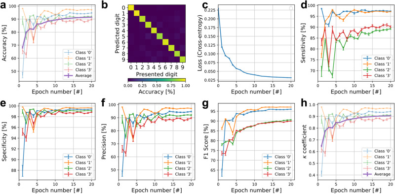
- For MNIST-style benchmarking, the paper uses a 60,000-image training set and 10,000-image test set; in the worked example, images are downsized from 28 × 28 to 8 × 8 and an ANN with one 64 × 10 single-layer perceptron is trained.
- In the example training study on 100 images, Scaled Conjugate Gradient and Levenberg–Marquardt achieved the highest accuracy, but Scaled Conjugate Gradient was chosen because it was faster.
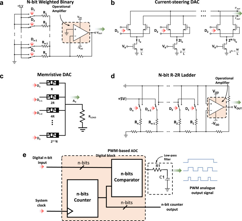
- The paper states that ADCs are often the largest and most power-hungry circuit block in memristive neural networks, consuming up to 70–90% of on-chip area and up to 80–88% of energy.
Methods
- Review/protocol article: synthesizes prior work on memristive ANN hardware and organizes the system into blocks (image capture, input driving, VMM core, sensing, activation, softargmax, ADCs, and training/update).
- Worked example: a single-layer perceptron for MNIST image classification; MATLAB is used to train the software model and generate a SPICE netlist, and SPICE simulation is used to evaluate the hybrid CMOS/memristor circuit during inference and write-verify programming.
- Analysis emphasis: compares ex situ vs in situ training, discusses conductance mapping to memristors, and surveys simulation abstraction levels from neural-network-level tools to circuit/SPICE-level models.
Limitations
- Stated in the paper: many published studies are not true full-hardware implementations; some only characterize a few devices or rely on software ANN simulations, so reported performance can be weakly connected to fabricated hardware.
- Stated in the paper: full on-chip memristive ANN implementation is limited by peripheral circuit overhead, ADC/DAC trade-offs, device non-idealities, and the difficulty of integrating memristor stacks with CMOS.
- Evident from the text: the paper is not an experimental validation of a new memristor ANN chip; it is primarily a review plus a simulation-based worked example, so its conclusions about performance are illustrative rather than a direct new hardware result.
Model-written summary. Check it against the paper before relying on it.
Integrity signals
Registry
Cites
Statistics
Figures






Verification
Claims the paper makes
47 Valid · 14 Not valid · 58 Not checked · 121 Own results and interpretations
At least one cited source doesn’t support this claim or points to a different paper, and none confirmed it — see the verdicts below.
In the paper
“ADCs with at least 8-bit resolution are necessary to achieve high (>90%) classification accuracy in a ResNET50-1.5 ANN used to classify the ImageNET157 database”
§ Hardware implementation of memristor-based artificial neural networks > Structure of memristor-based ANNs > Analogue to digital converters (Block 9)
What the sources say
- Disputedcites [157] Xiao, T. P. et al. On the Accuracy of Analog Neural Network Inference Accelerators. [Feature],” IEEE Circuits Syst. Mag. 22, 26–48 (2022). sourceExperimental — accuracy not yet measured
Section 6.3 (p. 12) says high accuracy is maintained with a 7-bit ADC, contrary to the claim that at least 8 bits are necessary. Table 2 in Section 4.3 (p. 7) reports 76.466% ImageNet top-1 accuracy for ResNet50-v1.5, not over 90%. (LLM, conf=0.93)
Checked by a reasoning model — may be wrong.
plainstates a cause- Asserted: passes — The authors put it forward as true.
- Checkable: passes — It can be checked against evidence.
- Load-bearing: unclear — It is unclear whether the paper’s conclusions depend on it.
- Based: passes — The paper gives a reason why it holds.
- Disputed
Some cited sources support this claim and some don’t — read each source’s verdict below.
In the paper
“the usual practice reported in the literature for this kind of training has been the use of the so-called Manhattan Update Rule105,194, or the Stochastic Gradient Descent54.”
§ Hardware implementation of memristor-based artificial neural networks > Structure of memristor-based ANNs > ANN training and synaptic weight update (Blocks 2, 11-15)
What the sources say
- Supportedcites [105] Prezioso, M. et al. “Training and operation of an integrated neuromorphic network based on metal-oxide memristors,”. Nature 521, 61–64 (2015). source
The Pattern Classification Experiment (p. 5) explicitly says the network was trained in situ using the Manhattan Update rule. This supports the Manhattan-rule example for which this paper is cited; the separate stochastic-gradient-descent citation is not being judged here. (LLM, conf=0.93)
- Disputedcites [194] Yao, P. et al., “Face classification using electronic synapses,” Nat. Commun., 8, May, 1–8, https://doi.org/10.1038/ncomms15199.2017, sourceExperimental — accuracy not yet measured
The citation to this paper is attached to the Stochastic Gradient Descent part of the sentence. In “RRAM-based neuromorphic network” (page unavailable), the paper calls its two weight-update rules the delta rule and the Manhattan rule; Figure 2’s caption explicitly says the demonstration uses a batch learning model, not stochastic gradient descent. (LLM, conf=0.83)
Checked by a reasoning model — may be wrong.
- Could not verifycites [54] Li, C. et al. “Efficient and self-adaptive in-situ learning in multilayer memristor neural networks,”. Nat. Commun. 9, 1–8 (2018). sourceExperimental — accuracy not yet measured
The Methods section describes ray-tracing simulations of bird-of-paradise feathers, not training memristor-based neural networks. Searches for the Manhattan Update Rule and stochastic gradient descent found no passage in our copy addressing either method as a usual training practice. (LLM, conf=0.78)
plain- Asserted: passes — The authors put it forward as true.
- Checkable: passes — It can be checked against evidence.
- Load-bearing: unclear — It is unclear whether the paper’s conclusions depend on it.
- Based: passes — The paper gives a reason why it holds.
- Supported
The cited sources support only part of this claim — read each source’s verdict below.
In the paper
“So far, several groups and companies have claimed the realization of hybrid CMOS/memristor implementations of ANNs53–61, —from now on, memristive ANNs— with performance that is superior to that of fully-CMOS counterparts.”
§ Hardware implementation of memristor-based artificial neural networks > Introduction
What the sources say
- Not checked — no full text of the sourcecites [53] Ishii, M. et al., “On-Chip Trainable 1.4M 6T2R PCM synaptic array with 1.6K Stochastic LIF neurons for spiking RBM,” Technical Digest - International Electron Devices Meeting, IEDM, 2019- 310–313, 2019, https://doi.org/10.1109/IEDM19573.2019.8993466. source
- Could not verifycites [54] Li, C. et al. “Efficient and self-adaptive in-situ learning in multilayer memristor neural networks,”. Nat. Commun. 9, 1–8 (2018). sourceExperimental — accuracy not yet measured
The Results section discusses super-black feather microstructure, and the Introduction discusses structural absorption of light; neither addresses artificial neural networks. Searches for hybrid CMOS/memristor implementations and performance relative to fully-CMOS systems found no relevant passage in our copy. (LLM, conf=0.78)
- Not checked — no full text of the sourcecites [55] Yao, P. et al. “Fully hardware-implemented memristor convolutional neural network,”. Nature 577, 641–646 (2020). source
- Not checked — no full text of the sourcecites [56] Correll, J. M. et al., “An 8-bit 20.7 TOPS/W Multi-Level Cell ReRAM-based Compute Engine,” in 2022 IEEE Symposium on VLSI Technology and Circuits (VLSI Technology and Circuits), IEEE, 264–265. https://doi.org/10.1109/VLSITechnologyandCir46769.2022.9830490.2022, source
- Not checked — no full text of the sourcecites [57] Cai, F. et al., “A fully integrated reprogrammable memristor-CMOS system for efficient multiply-accumulate operations,” Nat Electron, 2, no. July, 290–299, [Online]. Available: https://doi.org/10.1038/s41928-019-0270-x 2019. source
- Not checked — no full text of the sourcecites [58] Hung, J.-M., “An 8-Mb DC-Current-Free Binary-to-8b Precision ReRAM Nonvolatile Computing-in-Memory Macro using Time-Space-Readout with 1286.4-21.6TOPS/W for Edge-AI Devices,” in 2022 IEEE International Solid- State Circuits Conference (ISSCC), IEEE, 1–3. https://doi.org/10.1109/ISSCC42614.2022.9731715.2022, source
- Not checked — no full text of the sourcecites [59] Xue, C.-X., “15.4 A 22nm 2Mb ReRAM Compute-in-Memory Macro with 121-28TOPS/W for Multibit MAC Computing for Tiny AI Edge Devices,” in 2020 IEEE International Solid- State Circuits Conference - (ISSCC), IEEE, 2020, 244–246. source
- Partly supportedcites [60] Wan, W. et al. “A compute-in-memory chip based on resistive random-access memory,”. Nature 608, 504–512 (2022). sourceExperimental — accuracy not yet measured
The Main section describes NeuRRAM as an RRAM chip integrated with CMOS circuits and reports hardware-measured AI inference, supporting its use as an example of a hybrid implementation. The reported performance gains are against earlier RRAM compute-in-memory chips (Efficient voltage-mode neuron circuit), not fully-CMOS counterparts. The Methods section projects higher efficiency than edge inference accelerators only after scaling NeuRRAM from 130 nm to 7 nm; it does not establish the claimed superiority for the realized chip. (LLM, conf=0.84)
- Partly supportedcites [61] Yin, S., Sun, X., Yu, S. & Seo, J. S. “High-throughput in-memory computing for binary deep neural networks with monolithically integrated RRAM and 90-nm CMOS,”. IEEE Trans. Electron. Dev. 67, 4185–4192 (2020). sourceExperimental — accuracy not yet measured
The paper demonstrates a binary neural-network chip that integrates RRAM with 90-nm CMOS (p. 1), and its Results report a density advantage over SRAM-based in-memory computing (p. 6). But its quantified throughput and energy-delay improvements are compared with another CMOS chip containing embedded RRAM, not a fully-CMOS counterpart (Supplementary Figure 7, p. 32). It therefore supports the hybrid implementation, but not the claimed overall performance comparison with fully-CMOS ANNs. (LLM, conf=0.86)
plainstates an association- Asserted: passes — The authors put it forward as true.
- Checkable: passes — It can be checked against evidence.
- Load-bearing: unclear — It is unclear whether the paper’s conclusions depend on it.
- Based: passes — The paper gives a reason why it holds.
Every source the paper cites for this claim was checked and supports it.
In the paper
“Moreover, the switching time can be as short as 85 ps42.”
§ Hardware implementation of memristor-based artificial neural networks > Introduction
What the sources say
- Supportedcites [42] Choi, B. J. et al. “High-speed and low-energy nitride memristors,”. Adv. Funct. Mater. 26, 5290–5296 (2016). source
The Results and Discussion state that an AlN memristor switched both off and on in 85 ps. The Conclusions also report a measured ultrafast switching time of 85 ps in AlN memristors. (LLM, conf=0.95)
plain- Asserted: passes — The authors put it forward as true.
- Checkable: passes — It can be checked against evidence.
- Load-bearing: unclear — It is unclear whether the paper’s conclusions depend on it.
- Based: passes — The paper gives a reason why it holds.
- Supported
The cited sources support only part of this claim — read each source’s verdict below.
In the paper
“For instance, given the MNIST dataset in which images have a resolution of 28 × 28 pixels one option is to implement the synaptic layer using multiple crossbars to fit the 784 inputs (e.g., 13 64 × 64 or 4 256 × 256 crossbars would be needed93).”
§ Hardware implementation of memristor-based artificial neural networks > Structure of memristor-based ANNs > Image capture hardware (block 1) and input vector conformation (block 3)
What the sources say
- Partly supportedcites [93] Kim, H., Mahmoodi, M. R., Nili, H. & Strukov, D. B. “4K-memristor analog-grade passive crossbar circuit,”. Nat. Commun. 12, 1–11 (2021). sourceExperimental — accuracy not yet measured
The Results section (“Modeling of advanced systems”; page unavailable) supports splitting a 784-input MNIST classifier layer across multiple crossbar blocks. It does not give the claimed examples of 13 64 × 64 or 4 256 × 256 crossbars: its modeled implementation uses differential-pair weights and maps a 785 × 64 layer to 24 64 × 64 and two 17 × 64 blocks. (LLM, conf=0.88)
hedged- Asserted: passes — The authors put it forward as true.
- Checkable: passes — It can be checked against evidence.
- Load-bearing: unclear — It is unclear whether the paper’s conclusions depend on it.
- Based: passes — The paper gives a reason why it holds.
- Partly supported
88 more claims · 22 with their cited sources checked
Create a free account to see all 240 claims and to verify the 1 reference still open.
- Probably not a substantial claim. 79
- It may state two separate claims as one. 91
- The quote only partly states this claim. 1
Citations
Cites
Deep Residual Learning for Image Recognition
He, K., Zhang, X., Ren, S., & Sun, J. (2016) · 2016 IEEE Conference on Computer Vision and Pattern Recognition (CVPR) · doi:10.1109/cvpr.2016.90 · Cited by 235,474 · cited 1×
“For benchmarking a device or a chip, it is essential to evaluate the accuracy of standard deep neural network models like VGG 89 and ResNet 90 on CIFAR and ImageNet dataset by utilizing architecture-levelsimulationandrealistichardwarestatistics 91,92 .”
Very Deep Convolutional Networks for Large-Scale Image Recognition
Simonyan, K., & Zisserman, A. (2014) · arXiv · doi:10.48550/arxiv.1409.1556 · Cited by 114,148 · cited 1×
“For benchmarking a device or a chip, it is essential to evaluate the accuracy of standard deep neural network models like VGG 89 and ResNet 90 on CIFAR and ImageNet dataset by utilizing architecture-levelsimulationandrealistichardwarestatistics 91,92 .”
Adam: A Method for Stochastic Optimization
Kingma, D. P., & Ba, J. (2014) · arXiv · doi:10.48550/arxiv.1412.6980 · Cited by 98,946 · cited 2×
“…employed 165 , and for stochastic evaluation of the loss function using a mini-batch of images diverse methods have been employed, including Adaptive Gradient Algorithm (or AdaGrad) 182 , Root Mean Square Propagation (or RMSProp) 183 , Adaptive Moment Estimation (or Adam) 184 and Adadelta 185 .”
ImageNet: A large-scale hierarchical image database
Deng, J., Dong, W., Socher, R., Li, L.-J., Li, K., & Fei-Fei, L. (2009) · 2009 IEEE Conference on Computer Vision and Pattern Recognition · doi:10.1109/cvpr.2009.5206848 · Cited by 65,333 · cited 1×
“…86 ; 2) CIFAR (Canadian Institute for Advanced Research),whichcontains60,000colorimagesdividedinto10classes for CIFAR-10 and 100 classes for CIFAR-100 87 ; 3) ImageNet, one of the largest image datasets, which consists of over 1.2 million labelled from 1000 classes for the ImageNet competition 88 .”
InfluentialKennedy, J., & Eberhart, R. (2002) · Proceedings of ICNN'95 - International Conference on Neural Networks · doi:10.1109/icnn.1995.488968 · Cited by 58,192 · cited 1×
“Gradient-free methods such as the Particle Swarm optimization 168 , Genetic Algorithms 169 and Simulated Annealing 170 algorithms are more demanding from a computational point of view, andhence,theyarerarelyemployedforANNtraining,bywhichtheylie beyond the scope of this article.”
Optimization by Simulated Annealing
Kirkpatrick, S., Gelatt, C. D., & Vecchi, M. P. (1983) · Science · doi:10.1126/science.220.4598.671 · Cited by 45,134
Learning representations by back-propagating errors
Rumelhart, D. E., Hinton, G. E., & Williams, R. J. (1986) · Nature · doi:10.1038/323533a0 · Cited by 31,892 · cited 1×
“In most ANNs, the gradient of the loss function is normally computed by the backpropagation algorithm 171 .”
An Algorithm for Least-Squares Estimation of Nonlinear Parameters
Marquardt, D. W. (1963) · Journal of the Society for Industrial and Applied Mathematics · doi:10.1137/0111030 · Cited by 30,728 · cited 6×
“…evaluation, common optimization algorithms are the following: (i) Gradient Descent 165 (the simplest one and closest to the previous (cid:129) Manha(cid:3)an UpdateRule [181] (cid:129) Lavenberg-Marquardt[176] (cid:129) BFGS Quasi-Newton[172] Howdo we updatethe weightsduringeachitera(cid:2)on?”
InfluentialStrukov, D. B., Snider, G. S., Stewart, D. R., & Williams, R. S. (2008) · Nature · doi:10.1038/nature06932 · Cited by 11,828
(2017) · Cited by 11,625
Research works printed but not linked: 2
- “Microchips that mimic the human brain could make AI far more energy efficient | Science | AAAS.” Accessed: May 15, 2023. [Online]. Available: https://www.science.org/content/article/microchips-mimic-human-brain-could-make-ai-far-more-energy-efficient
- Ielmini, D. and Waser, R. Resistive Switching. Weinheim, Germany: Wiley-VCH Verlag GmbH & Co. KGaA, 2016.
Cited by
The growing memristor industry
Lanza, M., Pazos, S., Aguirre, F., Sebastian, A., Le Gallo, M., Alam, S. M., Ikegawa, S., Yang, J. J., Vianello, E., Chang, M.-F., et al. (2025) · Nature · doi:10.1038/s41586-025-08733-5 · Cited by 177
“…in purely passive, high-density 1R crossbar arrays 119 that can be self-rectifying 120 , but these alternatives are not demonstrated in commercial platforms, have limited size (64 × 64 memristors 119 ) and always require system-level mitigation of sneak-path currents 24 , adding complexity.”
Self-citationWeilenmann, C., Ziogas, A. N., Zellweger, T., Portner, K., Mladenović, M., Kaniselvan, M., Moraitis, T., Luisier, M., & Emboras, A. (2024) · Nature Communications · doi:10.1038/s41467-024-51093-3 · Cited by 147
“Although such investigations would certainly lead to increased energy consumption 59 , we believe that the memristor advantage is large enough (two orders of magnitude) to persist even under more realistic conditions.”
Synaptic and neural behaviours in a standard silicon transistor
Pazos, S. M., Zhu, K., Villena, M. A., Alharbi, O., Zheng, W., Shen, Y., Yuan, Y. J., Ping, Y., & Lanza, M. (2025) · Nature · doi:10.1038/s41586-025-08742-4 · Cited by 141
“…over a wide range of bursting frequencies and input stimuli (Supplementary Note 6), accommodate external reset signals (through bulk bias control pulsing) or operate as a two-, three-or four-terminal neuron in different neural network architectures 45 (Supplementary Note 6 and Supplementary Fig.”
Self-citationTwo-Dimensional Materials for Brain-Inspired Computing Hardware
Hadke, S. S., Kang, M., Sangwan, V. K., & Hersam, M. C. (2025) · Chemical Reviews · doi:10.1021/acs.chemrev.4c00631 · Cited by 110
Solution-processed memristors: performance and reliability
Pazos, S. M., Xu, X., Guo, T., Zhu, K., Alshareef, H. N., & Lanza, M. (2024) · Nature Reviews Materials · doi:10.1038/s41578-024-00661-6 · Cited by 107
“…would be the size of the crossbar array used for the neural network simulation based on the sizes of the memris-tors demonstrated — and note that this excludes all the peripheral circuitry such as digital-to-analog or analog-to-digital converters, transimpedance amplifiers and comparators 120 .”
Self-citation
Metadata
- Authors
- Aguirre, F., Sebastian, A., Le Gallo, M., Song, W., Wang, T., Yang, J. J., Lu, W., Chang, M.-F., Ielmini, D., Yang, Y., Mehonic, A., Kenyon, A., Villena, M. A., Roldán, J. B., Wu, Y., Hsu, H.-H., Raghavan, N., Suñé, J., Miranda, E., Eltawil, A., Setti, G., Smagulova, K., Salama, K. N., Krestinskaya, O., Yan, X., Ang, K.-W., Jain, S., Li, S., Alharbi, O., Pazos, S., & Lanza, M.
- Affiliations
- Universitat Autònoma de Barcelona (ES)
- IBM Research - Zurich (CH)
- University of Southern California (US)
- University of Michigan (US)
- National Tsing Hua University (TW)
- Consorzio Nazionale Interuniversitario per la Nanoelettronica (IT)
- Peking University (CN)
- University College London (GB)
- King Abdullah University of Science and Technology (SA)
- Universidad de Granada (ES)
- Singapore University of Technology and Design (SG)
- Hebei University (CN)
- National University of Singapore (SG)
- Corresponding author
- Lanza, Mario
- ORCID
- Aguirre, Fernando
- Sebastian, Abu
- Le Gallo, Manuel
- Song, Wenhao
- Wang, Tong
- Yang, J. Joshua
- Lu, Wei
- Chang, Meng-Fan
- Ielmini, Daniele
- Yang, Yuchao
- Mehonic, Adnan
- Kenyon, Anthony
- Villena, Marco A.
- Roldán, Juan B.
- Wu, Yuting
- Hsu, Hung-Hsi
- Raghavan, Nagarajan
- Suñé, Jordi
- Miranda, Enrique
- Eltawil, Ahmed
- Setti, Gianluca
- Smagulova, Kamilya
- Salama, Khaled N.
- Krestinskaya, Olga
- Yan, Xiaobing
- Ang, Kah-Wee
- Li, Sifan
- Alharbi, Osamah
- Pazos, Sebastian
- Lanza, Mario
- Venue
- Nature Communications
- Published
- 2024-03-04
- Volume
- 15
- Issue
- 1
- Pages
- 1974-1974
- ISSN
- 2041-1723 (ISSN-L)
- PMC
- PMC10912231
- OpenAlex
- W4392367648
- Cited by
- 564
- References
- 282
- Citations by year
- 2026: 246 · 2025: 247 · 2024: 71
- FWCI
- 11.53
- Type
- journal article
- Language
- en
- Open access
- gold
- doi.org
- Licence
- cc-by
- creativecommons.org/licenses/by/4.0 (tdm)
- creativecommons.org/licenses/by/4.0 (vor)
- Locations
- Nature Communications (publishedVersion, cc-by)
- PubMed Central (publishedVersion, cc-by)
- PubMed (publishedVersion)
- PORTO@Iris (submittedVersion, cc-by)
- National University of Singapore (submittedVersion, cc-by-nc-nd)
- RePEc: Research Papers in Economics (submittedVersion)
- DOAJ (DOAJ: Directory of Open Access Journals) (submittedVersion)
- UCL Discovery (University College London) (submittedVersion)
- Virtual Community of Pathological Anatomy (University of Castilla La Mancha) (submittedVersion)
- Greater South Information System
- Funders
- King Abdullah University of Science and Technology
- Universitat Autònoma de Barcelona
- Topics
- Physical Sciences › Engineering › Electrical and Electronic Engineering › Advanced Memory and Neural Computing
- Physical Sciences › Computer Science › Artificial Intelligence › Neural Networks and Applications
- Physical Sciences › Engineering › Electrical and Electronic Engineering › Ferroelectric and Negative Capacitance Devices
- Keywords
- memristors, hardware implementation, in-memory computing, neuromorphic hardware, energy efficiency, deep learning hardware, beyond-CMOS computing, performance estimation
About these checks
Registry, retraction, Cites and statistics results are computed, not judged, with one exception: a printed reference that no index lists is read once by a model before it counts as a citation error. Claims are extracted by a model and kept only when their quote appears verbatim in the text; each cited source is then checked, with a model’s help, for whether it says what the claim relies on. Those verdicts can be wrong — read the claim’s quote and the cited source before relying on one.
The claim verdicts this report counts are experimental: their accuracy is not yet measured.
A language model drew the claims from the paper on 2026-09-29, under version 3 of the claim definition (model deepseek-v4.1-flash, prompt extract-v3).
A second model labelled each claim on 2026-09-29 (model jev-1.13-20260917, definition revision gold-guideline-v0.2).
Cited sources are checked with a language model’s help (gpt-6-sol).
Statistics and arithmetic are recomputed, not judged.
Confidence bands are shown only for fields calibrated on our annotated test set. None is calibrated yet, so no band is shown.
What counts as a claim ›How we measure confidence ›How we check this ›
Are you an author, or do you see a problem with this page? Request a review
How to cite
Cite CoChat for the checks on this page, and the paper for its own findings.
- This page
- CoChat. (2026). Citation check: Hardware implementation of memristor-based artificial neural networks. https://app.cochat.ai/papers/10.1038/s41467-024-45670-9
- The paper
- Aguirre, F., Sebastian, A., Le Gallo, M., Song, W., Wang, T., Yang, J. J., Lu, W., Chang, M.-F., Ielmini, D., Yang, Y., Mehonic, A., Kenyon, A., Villena, M. A., Roldán, J. B., Wu, Y., Hsu, H.-H., Raghavan, N., Suñé, J., Miranda, E., . . . Lanza, M. (2024). Hardware implementation of memristor-based artificial neural networks. Nature Communications. https://doi.org/10.1038/s41467-024-45670-9
Data sources
Bibliographic data: Semantic Scholar, OpenAlex, Crossref.
Contains information from the Semantic Scholar Academic Graph Datasets, made available under the ODC Attribution License (ODC-BY 1.0).
Semantic Scholar’s data is described in: Kinney, R., et al. (2023). The Semantic Scholar Open Data Platform. arXiv:2301.10140.
