CoChat

2022 Roadmap on integrated quantum photonics

Open access

The DOI matches its Crossref record; 288 of the 288 references it cites were found in a registry or an index; 2 of the 3 sources its claims cite were checked for support.

Abstract

Abstract Integrated photonics will play a key role in quantum systems as they grow from few-qubit prototypes to tens of thousands of qubits. The underlying optical quantum technologies can only be realized through the integration of these components onto quantum photonic integrated circuits (QPICs) with accompanying electronics. In the last decade, remarkable advances in quantum photonic integration have enabled table-top experiments to be scaled down to prototype chips with improvements in efficiency, robustness, and key performance metrics. These advances have enabled integrated quantum photonic technologies combining up to 650 optical and electrical components onto a single chip that are capable of programmable quantum information processing, chip-to-chip networking, hybrid quantum system integration, and high-speed communications. In this roadmap article, we highlight the status, current and future challenges, and emerging technologies in several key research areas in integrated quantum photonics, including photonic platforms, quantum and classical light sources, quantum frequency conversion, integrated detectors, and applications in computing, communications, and sensing. With advances in materials, photonic design architectures, fabrication and integration processes, packaging, and testing and benchmarking, in the next decade we can expect a transition from single- and few-function prototypes to large-scale integration of multi-functional and reconfigurable devices that will have a transformative impact on quantum information science and engineering.

Overview

CoChat Summary

TL;DR

This roadmap surveys integrated quantum photonics, arguing that heterogeneous quantum photonic integrated circuits (QPICs) are needed to scale quantum systems from few-qubit prototypes to tens of thousands of qubits. It reviews platforms, light sources, frequency conversion, detectors, and applications, while identifying loss, integration, packaging, and foundry maturity as key challenges.

Key findings

  • Integrated quantum photonics has progressed from two-photon quantum interference in 2008 to devices combining more than 650 optical and electrical components capable of programmable two-qubit operations; conventional PICs today comprise ∼5 × 10³ components, so QPIC complexity still lags.
  • Heterogeneous integration is central: silicon photonics is the workhorse, but III-V, lithium niobate (LN/TFLN), SiC, diamond, Ta₂O₅, and AlGaAsOI platforms extend capabilities. Examples include AlGaAsOI entangled-pair generation >20 × 10⁹ pairs s⁻¹ mW⁻² near 1550 nm with heralded single-photon purity >99%, entanglement visibility >97%, and CAR >4300; TFLN waveguides with <3 dB m⁻¹ loss and 1.7 dB/facet coupling; and Ta₂O₅ waveguides with loss as low as 3 dB m⁻¹ and Q factors of several million.
  • Waveguide-integrated superconducting nanowire single-photon detectors (SNSPDs) achieve on-chip detection efficiencies >90%, <20 ps timing jitter, mHz dark counts, and maximum count rates exceeding 1 GHz; room-temperature APDs/SPADs are attractive but require improved dark counts and efficiency.
  • Applications span quantum computing, communications, sensing, quantum frequency conversion, and transduction, but require advances in low-loss switches, high-extinction modulation, integrated electronics, packaging, and foundry-compatible process design kits.

Methods

  • This is a multi-author roadmap article, not an original experimental study; it organizes status, current and future challenges, and advances across photonic platforms, quantum/classical light sources, quantum frequency conversion, integrated detectors, and applications.
  • The paper states: “No new data were created or analysed in this study.”
  • The main analysis is a qualitative synthesis of literature and expert perspectives, with figures and tables comparing platform and device performance metrics.

Limitations

  • The paper explicitly states that no new data were created or analysed.
  • As a roadmap, it is not a systematic review or meta-analysis; coverage is organized by invited sections and reflects the contributing authors’ perspectives.
  • The text makes evident that many field-level limitations remain, including QPIC complexity lagging conventional PICs, limited foundry maturity and PDKs for emerging platforms, and unresolved challenges in loss, noise, yield, packaging, and cryogenic operation.

Model-written summary. Check it against the paper before relying on it.

Integrity signals

Registry

Crossref · 10.1088/2515-7647/ac1ef4

Cites

288 of 288 references verified0 citation errors · 0 not checkable

Statistics

Nothing to recompute.

Figures

Image 1
From the PDF
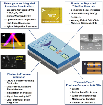
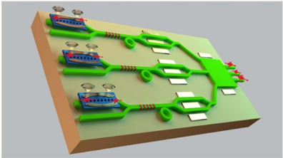
Figure 3 Heterogeneous integrated photonic platform. Inserts depict elements developed at MIT LL: (a) 3D beam profiles from multi-wavelength surface-grating lenses for trapped-ion illumination, (b) TFLN bonded to silicon-nitride ring resonators, (c) InGaAsP/InP quantum-well membrane bonded to silicon dioxide with InP regrowth, (d) flip-chipped semiconductor optical amplifiers, and (e) single-photon Geiger-mode APDs (GmAPDs). Panel (a) reprinted with permission from Springer Nature. Panel (b) reprinted with permission from [20]. Panel (d) reprinted with permission from [17] under a Creative Commons License.
Figure 3 Heterogeneous integrated photonic platform. Inserts depict elements developed at MIT LL: (a) 3D beam profiles from multi-wavelength surface-grating lenses for trapped-ion illumination, (b) TFLN bonded to silicon-nitride ring resonators, (c) InGaAsP/InP quantum-well membrane bonded to silicon dioxide with InP regrowth, (d) flip-chipped semiconductor optical amplifiers, and (e) single-photon Geiger-mode APDs (GmAPDs). Panel (a) reprinted with permission from Springer Nature. Panel (b) reprinted with permission from [20]. Panel (d) reprinted with permission from [17] under a Creative Commons License.From the PDF
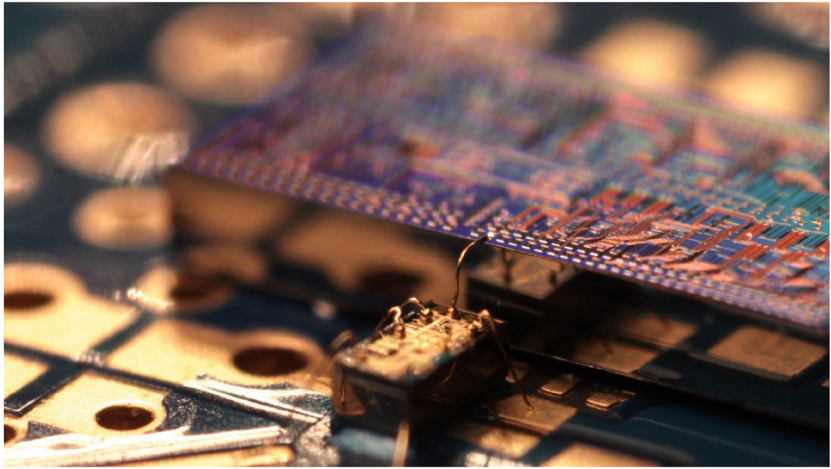
Figure 4 An integrated electronics die directly wire-bonded with a silicon photonics integrated circuit reduces total device capacitance, thereby enabling in this instance [33] a high bandwidth homodyne detection for squeezed light detection on-chip (Photo credit: Joel Tasker, University of Bristol).
Figure 4 An integrated electronics die directly wire-bonded with a silicon photonics integrated circuit reduces total device capacitance, thereby enabling in this instance [33] a high bandwidth homodyne detection for squeezed light detection on-chip (Photo credit: Joel Tasker, University of Bristol).From the PDF
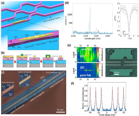
Figure 5 Heterogenous integration for single QD devices. (a) Schematic of SiN waveguide-based quantum photonic circuits with directly integrated SPSs. As shown in the inset, the sources are GaAs-based nanophotonic geometries (here a straight waveguide with adiabatic mode transformers) that host single QDs, which can be triggered to emit single-photons at a time. (b) Possible process flow for the geometry in (a). (b) False-color scanning electron micrograph of fabricated SiN-coupled SPS as in (a). (d) Emission spectrum and second-order correlation for a single QD in the device in (c), indicating single-photon emission [40]. (e) While in (c) the QDs were randomly located within the GaAs waveguides, in [41] cathodoluminescence (CL) images were used to identify single QDs before fabrication (top left). The CL image was used to deterministically produce the waveguide shown on the right-hand side around the located QD with high precision, as evidenced in the post-fab CL map. (f) Second-order correlation of light emission from the QD in (e), where the strong anti-bunching at zero time delay indicated pure, triggered single-photon emission into the SiN waveguide [41]. Panels (a)-(d) reprinted with permission from [40]. Panels (e) and (f) reprinted with permission from [41], © 2019 American Chemical Society.
Figure 5 Heterogenous integration for single QD devices. (a) Schematic of SiN waveguide-based quantum photonic circuits with directly integrated SPSs. As shown in the inset, the sources are GaAs-based nanophotonic geometries (here a straight waveguide with adiabatic mode transformers) that host single QDs, which can be triggered to emit single-photons at a time. (b) Possible process flow for the geometry in (a). (b) False-color scanning electron micrograph of fabricated SiN-coupled SPS as in (a). (d) Emission spectrum and second-order correlation for a single QD in the device in (c), indicating single-photon emission [40]. (e) While in (c) the QDs were randomly located within the GaAs waveguides, in [41] cathodoluminescence (CL) images were used to identify single QDs before fabrication (top left). The CL image was used to deterministically produce the waveguide shown on the right-hand side around the located QD with high precision, as evidenced in the post-fab CL map. (f) Second-order correlation of light emission from the QD in (e), where the strong anti-bunching at zero time delay indicated pure, triggered single-photon emission into the SiN waveguide [41]. Panels (a)-(d) reprinted with permission from [40]. Panels (e) and (f) reprinted with permission from [41], © 2019 American Chemical Society.From the PDF
Figure 6 Demonstrations on (Al)GaAsOI platform. (a) Scanning electron microscopy (SEM) image of the cross section of an AlGaAsOI waveguide. (b) Transmission spectrum of an AlGaAs resonator. The extracted Q is 3.3 × 10 6 . (c) The transfer function of SHG normalized efficiency for a GaAsOI waveguide. (d) SHG spectrums under different temperatures by a GaAsOI waveguide, whose normalized efficiency is >40 000% W -1 cm -2 . (e) The generated frequency comb lines from an AlGaAs resonator under 23 µ Wpower. (f) Frequency conversion for communication experiment by an AlGaAsOI waveguide. Panel (a) reprinted with permission from [45]. Panel (d) reprinted with permission from [48]. Panel (e) reprinted with permission from [47]. Panel (f) reprinted with permission from [49].
Figure 6 Demonstrations on (Al)GaAsOI platform. (a) Scanning electron microscopy (SEM) image of the cross section of an AlGaAsOI waveguide. (b) Transmission spectrum of an AlGaAs resonator. The extracted Q is 3.3 × 10 6 . (c) The transfer function of SHG normalized efficiency for a GaAsOI waveguide. (d) SHG spectrums under different temperatures by a GaAsOI waveguide, whose normalized efficiency is >40 000% W -1 cm -2 . (e) The generated frequency comb lines from an AlGaAs resonator under 23 µ Wpower. (f) Frequency conversion for communication experiment by an AlGaAsOI waveguide. Panel (a) reprinted with permission from [45]. Panel (d) reprinted with permission from [48]. Panel (e) reprinted with permission from [47]. Panel (f) reprinted with permission from [49].From the PDF
Image 6
From the PDF
Image 7
From the PDF
Image 8
From the PDF
Figure 10 (a) Single-soliton frequency comb output spectrum from an air-clad Ta2O5-micro-ring resonator (1.6 µ mwidth, 570 nm height, 46 µ mradius). (b) Supercontinuum generation in oxide-clad Ta2O5-waveguides (1.45 µ mwidth, 800 nm height, 5 mm length) as a function of input laser power. Panel (a) reprinted with permission from [64], panel (b) reprinted with permission from [65].
Figure 10 (a) Single-soliton frequency comb output spectrum from an air-clad Ta2O5-micro-ring resonator (1.6 µ mwidth, 570 nm height, 46 µ mradius). (b) Supercontinuum generation in oxide-clad Ta2O5-waveguides (1.45 µ mwidth, 800 nm height, 5 mm length) as a function of input laser power. Panel (a) reprinted with permission from [64], panel (b) reprinted with permission from [65].From the PDF
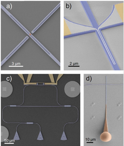
Figure 11 Nanophotonic circuit components for Ta2O5-on-insulator: (a) nanodiamonds (orange) containing quantum emitters coupled to 1D-photonic crystal cavities (blue) in Ta2O5-waveguides for optical excitation and single-photon collection. (b) Ta2O5-waveguide-integrated SNSPD (white). (c) Opto-electromechanical phase shifter (top) embedded in a Mach-Zehnder interferometer formed by multimode interference devices (center) accessible from optical fibers via grating couplers (bottom). (d) Total internal reflection coupler (orange) produced in 3D direct laser writing, providing an efficient optical interface to Ta2O5-waveguides (blue). Panel (b) reprinted with permission from [70] under a Creative Commons Attribution 4.0 International License. Panel (c) reprinted with permission from [71].
Figure 11 Nanophotonic circuit components for Ta2O5-on-insulator: (a) nanodiamonds (orange) containing quantum emitters coupled to 1D-photonic crystal cavities (blue) in Ta2O5-waveguides for optical excitation and single-photon collection. (b) Ta2O5-waveguide-integrated SNSPD (white). (c) Opto-electromechanical phase shifter (top) embedded in a Mach-Zehnder interferometer formed by multimode interference devices (center) accessible from optical fibers via grating couplers (bottom). (d) Total internal reflection coupler (orange) produced in 3D direct laser writing, providing an efficient optical interface to Ta2O5-waveguides (blue). Panel (b) reprinted with permission from [70] under a Creative Commons Attribution 4.0 International License. Panel (c) reprinted with permission from [71].From the PDF
Figure 12 Integrated TFLN photonics. (a) Ultra-low loss (3 dB m -1 ) optical waveguides and highQ resonators (Q ∼ 10 000 000). (b) Microwave-to-optical transducer. (c) Periodically poled TFLN frequency converter. (d) Efficient and wideband EOM. Panels (a)-(c) reprinted with permission from [73], [79] and [75], respectively. Panel (d) reprinted from [74] with permission from Springer Nature.
Figure 12 Integrated TFLN photonics. (a) Ultra-low loss (3 dB m -1 ) optical waveguides and highQ resonators (Q ∼ 10 000 000). (b) Microwave-to-optical transducer. (c) Periodically poled TFLN frequency converter. (d) Efficient and wideband EOM. Panels (a)-(c) reprinted with permission from [73], [79] and [75], respectively. Panel (d) reprinted from [74] with permission from Springer Nature.From the PDF
Figure 13 Multiplexed quantum repeater node in LN that combines diamond quantum memories with low-loss nonlinear photonics.
Figure 13 Multiplexed quantum repeater node in LN that combines diamond quantum memories with low-loss nonlinear photonics.From the PDF
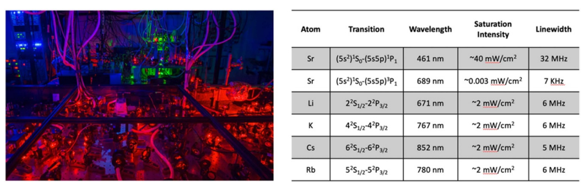
Figure 14 (Left) Atom-based experiments in quantum science like this lithium quantum gas apparatus typically utilize benchtop equipment and free-space optics which dominate the cost and complexity and restrict scalability. (Right) Properties of some atomic transitions of general interest.
Figure 14 (Left) Atom-based experiments in quantum science like this lithium quantum gas apparatus typically utilize benchtop equipment and free-space optics which dominate the cost and complexity and restrict scalability. (Right) Properties of some atomic transitions of general interest.From the PDF
Figure 15 (a) Summary of laser technologies on silicon (GeOI-germanium on insulator, SOI-silicon on insulator, SNOI-silicon-nitride on insulator, R stands for one or more rings), (b) automated wafer scale testing of lasers captured with operation Si camera showing light emission below Si bandgap, (c) exemplary LIV curves showing very good laser performance (the wavelength of is 980 nm) and (d) heterogeneous GaAs-on-SiN wafer with multiple active components including lasers, amplifiers, photodetectors and tuners.
Figure 15 (a) Summary of laser technologies on silicon (GeOI-germanium on insulator, SOI-silicon on insulator, SNOI-silicon-nitride on insulator, R stands for one or more rings), (b) automated wafer scale testing of lasers captured with operation Si camera showing light emission below Si bandgap, (c) exemplary LIV curves showing very good laser performance (the wavelength of is 980 nm) and (d) heterogeneous GaAs-on-SiN wafer with multiple active components including lasers, amplifiers, photodetectors and tuners.From the PDF
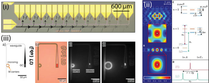
Figure 17 (i) Cryogenic optical link between electrically-injected waveguide-coupled W center LED and SNSPDs. Reprinted from [115], with the permission of AIP Publishing. (ii) Proposed spin-photon interface in silicon. Reprinted with permission from [119], under a Creative Commons Attribution 4.0 International License. (iii) Demonstrated coupling of W centers to
Figure 17 (i) Cryogenic optical link between electrically-injected waveguide-coupled W center LED and SNSPDs. Reprinted from [115], with the permission of AIP Publishing. (ii) Proposed spin-photon interface in silicon. Reprinted with permission from [119], under a Creative Commons Attribution 4.0 International License. (iii) Demonstrated coupling of W centers toFrom the PDF
Figure 18 SiC lattice illustrated in a shape of a (technology) backbone hosting different types of defects with examples of applications in integrated nanodevices. Integrated qubits subfigure was adapted with permission from [123], © 2020 American Chemical Society. Spin-photon entanglement subfigure was adapted with permission from [127], © 2020 by the American Physical Society.
Figure 18 SiC lattice illustrated in a shape of a (technology) backbone hosting different types of defects with examples of applications in integrated nanodevices. Integrated qubits subfigure was adapted with permission from [123], © 2020 American Chemical Society. Spin-photon entanglement subfigure was adapted with permission from [127], © 2020 by the American Physical Society.From the PDF
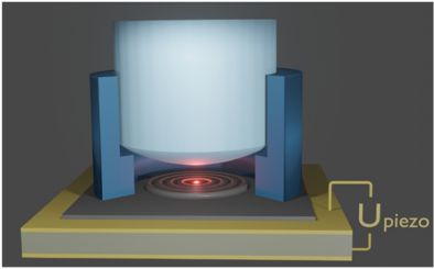
Figure 19 Schematic view of an 'ideal' telecom wavelength SPS. The on-chip fiber coupled quantum device includes a single quantum emitter integrated deterministically into a CBG structure with backside gold mirror and a piezo element for spectral control. Reprinted by courtesy of Sven Rodt, Technische Universität Berlin.
Figure 19 Schematic view of an 'ideal' telecom wavelength SPS. The on-chip fiber coupled quantum device includes a single quantum emitter integrated deterministically into a CBG structure with backside gold mirror and a piezo element for spectral control. Reprinted by courtesy of Sven Rodt, Technische Universität Berlin.From the PDF
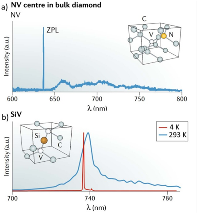
Figure 20 Fluorescence spectra of the two most prominent diamond color centers. (a) The negatively charged NV center displays a sharp ZPL amounting to 4% of the total emission at 4K, with the rest corresponding to the broad phonon sideband. (b) The negatively charged SiV center has 70%-80% of its emission into the ZPL. Among the dozens of known diamond color centers these two are the most studied, as they offer long-lived, optically-accessible spin qubits. The structures of the color centers (insets) explain the differences between their properties. The inversion symmetry of the SiV reduces its sensitivity to stray electric fields but also introduces increased sensitivity to thermal phonons. Other group IV color centers such as the germanium- (GeV) and tin- (SnV) vacancy centers share the structure of the SiV, making them promising candidates for further study [151]. (a) and (b) are reprinted with permission from [58], © Springer Nature 2018.
Figure 20 Fluorescence spectra of the two most prominent diamond color centers. (a) The negatively charged NV center displays a sharp ZPL amounting to 4% of the total emission at 4K, with the rest corresponding to the broad phonon sideband. (b) The negatively charged SiV center has 70%-80% of its emission into the ZPL. Among the dozens of known diamond color centers these two are the most studied, as they offer long-lived, optically-accessible spin qubits. The structures of the color centers (insets) explain the differences between their properties. The inversion symmetry of the SiV reduces its sensitivity to stray electric fields but also introduces increased sensitivity to thermal phonons. Other group IV color centers such as the germanium- (GeV) and tin- (SnV) vacancy centers share the structure of the SiV, making them promising candidates for further study [151]. (a) and (b) are reprinted with permission from [58], © Springer Nature 2018.From the PDF
Figure 21 Example structure of a quantum network node. (a) Schematic of the experimental setup used in [147]. SiV centers are embedded in a nanophotonic cavity, surrounded by gold coplanar waveguides for spin control. Photons produced by the color centers are collected through the tapered fiber interface at the end of the device. (b) SEM image of the device shown in panel (a) inset shows the nanophotonic crystal cavity. (c) Schematic representation of a general quantum repeater node. A pair of quantum emitters inside cavities are placed at each node. The nature of the emitters and cavities varies depending on the platform used. After successfully heralding entanglement with adjacent nodes, Bell-state measurements are performed between the memories in the two cavities to teleport entanglement to the distant nodes. (a) and (b) are reprinted with permission from Nguyen C T et al 2019 Phys. Rev. Lett. 123 183602, © 2019 by the American Physical Society. (c) is reprinted from Nemoto K et al 2016 Sci. Rep. 6 26284, under a Creative Commons Attribution 4.0 International License
Figure 21 Example structure of a quantum network node. (a) Schematic of the experimental setup used in [147]. SiV centers are embedded in a nanophotonic cavity, surrounded by gold coplanar waveguides for spin control. Photons produced by the color centers are collected through the tapered fiber interface at the end of the device. (b) SEM image of the device shown in panel (a) inset shows the nanophotonic crystal cavity. (c) Schematic representation of a general quantum repeater node. A pair of quantum emitters inside cavities are placed at each node. The nature of the emitters and cavities varies depending on the platform used. After successfully heralding entanglement with adjacent nodes, Bell-state measurements are performed between the memories in the two cavities to teleport entanglement to the distant nodes. (a) and (b) are reprinted with permission from Nguyen C T et al 2019 Phys. Rev. Lett. 123 183602, © 2019 by the American Physical Society. (c) is reprinted from Nemoto K et al 2016 Sci. Rep. 6 26284, under a Creative Commons Attribution 4.0 International LicenseFrom the PDF
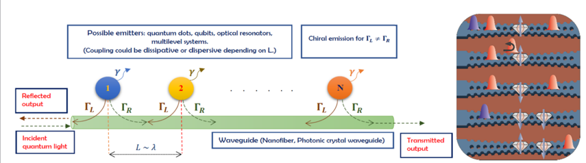
Figure 22 (Left) Model of a string of N quantum emitters side-coupled to a 1D continuum. (Right) An on-chip integrated-waveguide quantum gate with color-center nanodiamonds; the blue and red colours represent single photons of different frequencies, with output dependent on the state of the color center.
Figure 22 (Left) Model of a string of N quantum emitters side-coupled to a 1D continuum. (Right) An on-chip integrated-waveguide quantum gate with color-center nanodiamonds; the blue and red colours represent single photons of different frequencies, with output dependent on the state of the color center.From the PDF
Figure 23 Potential use for QFC in a quantum network consisting of nodes based on spins that are optically addressable at a visible frequency ω 1. QFC to and from a telecom frequency ω 2 can help mediate photonic connections between spins over a fiber optic network. Here, a nanophotonic QFC interface such as that from [177] is depicted. The table shows typical 3 dB attenuation lengths for single mode optical fiber (SMF) at different wavelengths, highlighting the benefits of telecom-band operation.
Figure 23 Potential use for QFC in a quantum network consisting of nodes based on spins that are optically addressable at a visible frequency ω 1. QFC to and from a telecom frequency ω 2 can help mediate photonic connections between spins over a fiber optic network. Here, a nanophotonic QFC interface such as that from [177] is depicted. The table shows typical 3 dB attenuation lengths for single mode optical fiber (SMF) at different wavelengths, highlighting the benefits of telecom-band operation.From the PDF
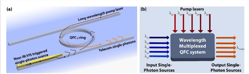
Figure 24 Representative opportunities enabled by integrated nanophotonic QFC systems. (a) Heterogeneous integration of a triggered SPS (bottom left, in yellow) with a telecom QFC interface. Single photons (for example, generated by an InAs QD in a GaAs waveguide) are efficiently transferred into the QFC device layer (gray), where they are combined with a long wavelength pump laser (dark red arrow) to generate telecom-band single photons (orange). (b) Wavelength-multiplexed QFC system in which input SPSs at different wavelengths ( λ s1,…, λ s5) are combined with appropriate pump lasers ( λ p1,…, λ p5) to yield identical output telecom SPSs at wavelength λ t -com. The QFC system could consist of many separate devices, each tailored for a specific λ s / λ p/ λ t -com configuration, or a single device that can operate on a broad range of input wavelengths and has been engineered to inhibit competitive multi-pump processes. Such a device could enable other operations as well, for example, translating the input single photons to distinct output wavelengths using a single pump. Advances in heterogeneous integration, for example through transfer printing and pick-and-place approaches, suggest that both the SPSs and pump lasers (as well as auxiliary components not shown, such as filters and couplers) can be integrated with the QFC device(s) into a single photonic platform.
Figure 24 Representative opportunities enabled by integrated nanophotonic QFC systems. (a) Heterogeneous integration of a triggered SPS (bottom left, in yellow) with a telecom QFC interface. Single photons (for example, generated by an InAs QD in a GaAs waveguide) are efficiently transferred into the QFC device layer (gray), where they are combined with a long wavelength pump laser (dark red arrow) to generate telecom-band single photons (orange). (b) Wavelength-multiplexed QFC system in which input SPSs at different wavelengths ( λ s1,…, λ s5) are combined with appropriate pump lasers ( λ p1,…, λ p5) to yield identical output telecom SPSs at wavelength λ t -com. The QFC system could consist of many separate devices, each tailored for a specific λ s / λ p/ λ t -com configuration, or a single device that can operate on a broad range of input wavelengths and has been engineered to inhibit competitive multi-pump processes. Such a device could enable other operations as well, for example, translating the input single photons to distinct output wavelengths using a single pump. Advances in heterogeneous integration, for example through transfer printing and pick-and-place approaches, suggest that both the SPSs and pump lasers (as well as auxiliary components not shown, such as filters and couplers) can be integrated with the QFC device(s) into a single photonic platform.From the PDF
Figure 25 (a) A χ (2) cavity with single-photon nonlinearity based on a periodically pole LN microring and its schematic energy level diagram (right panel). The anharmonicity of the nonlinear system is determined by the energy level splitting relative to their widths. (b) The coupling rate g , dissipation rate κ as well as the corresponding single-photon nonlinearity FOM demonstrated in various integrated χ (2) cavities. µ ring, microring; PhC, photonic crystal. Reprinted with permission from [189].
Figure 25 (a) A χ (2) cavity with single-photon nonlinearity based on a periodically pole LN microring and its schematic energy level diagram (right panel). The anharmonicity of the nonlinear system is determined by the energy level splitting relative to their widths. (b) The coupling rate g , dissipation rate κ as well as the corresponding single-photon nonlinearity FOM demonstrated in various integrated χ (2) cavities. µ ring, microring; PhC, photonic crystal. Reprinted with permission from [189].From the PDF
Figure 26 Device concepts for SNSPDs coupled to PICs. U- or W-shaped SNSPD coupled to a single waveguide (yellow). Multiple SNSPDs on a single waveguide or an array of waveguides (blue). SNSPDs coupled to 1D and 2D cavities (green).
Figure 26 Device concepts for SNSPDs coupled to PICs. U- or W-shaped SNSPD coupled to a single waveguide (yellow). Multiple SNSPDs on a single waveguide or an array of waveguides (blue). SNSPDs coupled to 1D and 2D cavities (green).From the PDF
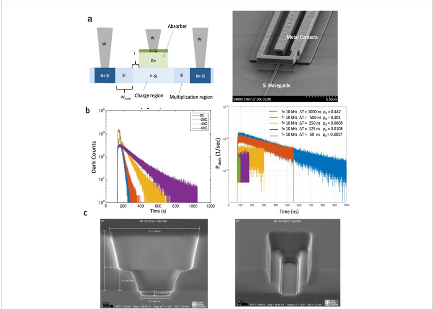
Figure 27 (a) (Left) Schematic of lateral Ge on Si SACM APD and (right) top-down view of waveguide coupled SACM with oxide cladding removed. (b) (Left) Measured dark counts of SACM APD for various operating temperatures and (right) dark count probability for fixed repetition rate with variable gate duration. (c) SEM template for aspect ratio trapped growth of Ge on Si for reduction of defects and improved dark count rate. Reprinted with permission from [212].
Figure 27 (a) (Left) Schematic of lateral Ge on Si SACM APD and (right) top-down view of waveguide coupled SACM with oxide cladding removed. (b) (Left) Measured dark counts of SACM APD for various operating temperatures and (right) dark count probability for fixed repetition rate with variable gate duration. (c) SEM template for aspect ratio trapped growth of Ge on Si for reduction of defects and improved dark count rate. Reprinted with permission from [212].From the PDF
Figure 28 Resonant GeSn waveguide-coupled SACM APD design with Si epi multiplication region on top. Right figure shows GeSN APD array for through Si illumination or waveguide coupling.
Figure 28 Resonant GeSn waveguide-coupled SACM APD design with Si epi multiplication region on top. Right figure shows GeSN APD array for through Si illumination or waveguide coupling.From the PDF
Figure 29 Integrated optical architecture for trapped-ion quantum control, as described and with some elements realized in [10, 15, 222-224]. Tan (gray) electrodes, transparent here for clarity, are for production of RF (DC) components of the trapping potential. Photonic elements in layers below the electrodes include single-mode waveguides and splitters, modulators for switching and frequency control, grating couplers for control-light emission or photon collection (possibly into multi-mode waveguides), and single-photon detectors for ion-qubit state determination. Control electronics could be in a lower layer or in a separate, bonded substrate.
Figure 29 Integrated optical architecture for trapped-ion quantum control, as described and with some elements realized in [10, 15, 222-224]. Tan (gray) electrodes, transparent here for clarity, are for production of RF (DC) components of the trapping potential. Photonic elements in layers below the electrodes include single-mode waveguides and splitters, modulators for switching and frequency control, grating couplers for control-light emission or photon collection (possibly into multi-mode waveguides), and single-photon detectors for ion-qubit state determination. Control electronics could be in a lower layer or in a separate, bonded substrate.From the PDF
Figure 30 Two d -dimensional qudits can be encoded a single photon using time bins and frequency. Arbitrary superpositions of different time and frequency bins can be encoded (unused time-frequency slots are shown as dashed circles). Deterministic quantum operations can be performed on the two-qudit state such that the orientation of the time-frequency superpositions is changed, hence creating a new two-qudit state. This approach gets rid of the multiphoton interaction usually required for this kind of operation. Reprinted with permission from [233].
Figure 30 Two d -dimensional qudits can be encoded a single photon using time bins and frequency. Arbitrary superpositions of different time and frequency bins can be encoded (unused time-frequency slots are shown as dashed circles). Deterministic quantum operations can be performed on the two-qudit state such that the orientation of the time-frequency superpositions is changed, hence creating a new two-qudit state. This approach gets rid of the multiphoton interaction usually required for this kind of operation. Reprinted with permission from [233].From the PDF
Figure 31 Transverse spatial modes in a multi-mode waveguide (a) can exhibit Hong-Ou-Mandel two-photon interference (b). A chip implementation (c) is achieved through spatial mode multiplexing via asymmetric directional couplers and spatial mode beamsplitters via nanoscale gratings. The mode order within the multi-mode region is indicated by the colours (red is TE0, green is TE2) indicate the mode order of the device. The inset shows a microscope image, scale bar is 160 µ m. Reprinted with permission from [235].
Figure 31 Transverse spatial modes in a multi-mode waveguide (a) can exhibit Hong-Ou-Mandel two-photon interference (b). A chip implementation (c) is achieved through spatial mode multiplexing via asymmetric directional couplers and spatial mode beamsplitters via nanoscale gratings. The mode order within the multi-mode region is indicated by the colours (red is TE0, green is TE2) indicate the mode order of the device. The inset shows a microscope image, scale bar is 160 µ m. Reprinted with permission from [235].From the PDF
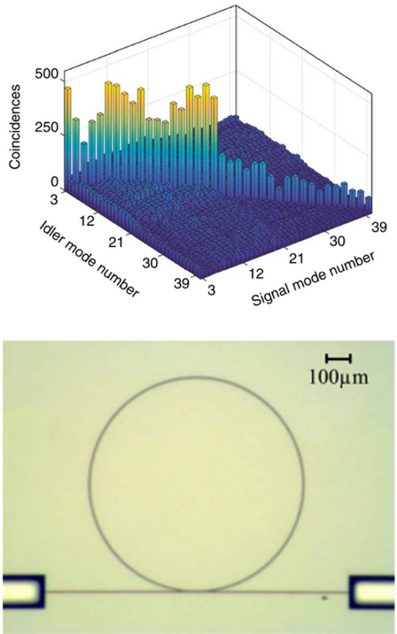
Figure 32 (Top) JSI showing spectral correlations between signal and idler photons across 30 + modes. (Bottom) Microscope image of the microring and U-grooves to support fiber coupling. Reprinted with permission from [240].
Figure 32 (Top) JSI showing spectral correlations between signal and idler photons across 30 + modes. (Bottom) Microscope image of the microring and U-grooves to support fiber coupling. Reprinted with permission from [240].From the PDF
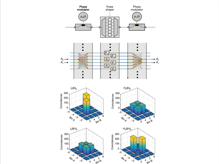
Figure 33 (Top) Concept illustration for a three-element quantum frequency processor. The physical configuration comprises phase modulators and a central pulse shaper. (Bottom) Measured correlations of a two-qubit frequency-bin entangled state, where each qubit is operated on by either the identity ( I ) or Hadamard ( H ) gates independently. Reprinted with permission from [68], © Springer Nature 2019.
Figure 33 (Top) Concept illustration for a three-element quantum frequency processor. The physical configuration comprises phase modulators and a central pulse shaper. (Bottom) Measured correlations of a two-qubit frequency-bin entangled state, where each qubit is operated on by either the identity ( I ) or Hadamard ( H ) gates independently. Reprinted with permission from [68], © Springer Nature 2019.From the PDF
Figure 34 (a) Schematic for the generation of a 1D cluster state [250], where p and q squeezed vacua are interfered creating a series of EPR states every time constant ∆ t . One spatial mode of the EPR state is delayed by one time constant forming a dual rail cluster state which is represented by (a) and (b) linear chain of temporal modes. Extending the 1D scheme with a second set of squeezers and delay of length N ∆ t forms (a) and (c) 2D cluster state with a square lattice shape, which is the primary resource for CV-MBQC. Circuit for 2D cluster state shown figure 35. Blue circles indicate temporal modes, yellow circles are GKP states inserted into the cluster for error correction or non-Gaussian operations. Red arrow shows the flow of information encoded in the input states down the chain (cluster) for 1D (2D) cluster states. BS-beam splitter, HD-homodyne detector, LO-local oscillator.
Figure 34 (a) Schematic for the generation of a 1D cluster state [250], where p and q squeezed vacua are interfered creating a series of EPR states every time constant ∆ t . One spatial mode of the EPR state is delayed by one time constant forming a dual rail cluster state which is represented by (a) and (b) linear chain of temporal modes. Extending the 1D scheme with a second set of squeezers and delay of length N ∆ t forms (a) and (c) 2D cluster state with a square lattice shape, which is the primary resource for CV-MBQC. Circuit for 2D cluster state shown figure 35. Blue circles indicate temporal modes, yellow circles are GKP states inserted into the cluster for error correction or non-Gaussian operations. Red arrow shows the flow of information encoded in the input states down the chain (cluster) for 1D (2D) cluster states. BS-beam splitter, HD-homodyne detector, LO-local oscillator.From the PDF
Figure 35 Artistic impression of a PIC for the generation of 2D cluster state based the design of [247]. Photonic circuit features periodic poling for generation of squeezed vacua, tunable beamsplittters, on-chip delay lines and homodyne detection. Using an optical switch prepared GKP states can be injected into the cluster to provide error-correction and non-Gaussian operations.
Figure 35 Artistic impression of a PIC for the generation of 2D cluster state based the design of [247]. Photonic circuit features periodic poling for generation of squeezed vacua, tunable beamsplittters, on-chip delay lines and homodyne detection. Using an optical switch prepared GKP states can be injected into the cluster to provide error-correction and non-Gaussian operations.From the PDF
Image 34
From the PDF
Image 35
From the PDF

Verification

Claims the paper makes

2 Valid · 6 Not valid · 1 Not checked · 3 Own results and interpretations

7 more claims

Create a free account to see all 12 claims and every source verdict.

See all claims — free account

Citations

Cites

Show all 288 references

Research works printed but not linked: 1

  1. Juanjuan, 2020, Towards 1% single photon nonlinearity with periodically-poled lithium niobate microring resonators, Optica, 7, 1654, 10.1364/OPTICA.403931 · DOI · Paper page

Cited by

See all 11

Metadata

Authors
Moody, G., Sorger, V. J., Blumenthal, D. J., Juodawlkis, P. W., Loh, W., Sorace-Agaskar, C., Jones, A. E., Balram, K. C., Matthews, J. C. F., Laing, A., Davanco, M., Chang, L., Bowers, J. E., Quack, N., Galland, C., Aharonovich, I., Wolff, M. A., Schuck, C., Sinclair, N., Lončar, M., Komljenovic, T., Weld, D., Mookherjea, S., Buckley, S., Radulaski, M., Reitzenstein, S., Pingault, B., Machielse, B., Mukhopadhyay, D., Akimov, A., Zheltikov, A., Agarwal, G. S., Srinivasan, K., Lu, J., Tang, H. X., Jiang, W., McKenna, T. P., Safavi-Naeini, A. H., Steinhauer, S., Elshaari, A. W., Zwiller, V., Davids, P. S., Martinez, N., Gehl, M., Chiaverini, J., Mehta, K. K., Romero, J., Lingaraju, N. B., Weiner, A. M., Peace, D., Cernansky, R., Lobino, M., Diamanti, E., Vidarte, L. T., & Camacho, R. M.
Affiliations
  • University of California, Santa Barbara (US)
  • George Washington University (US)
  • MIT Lincoln Laboratory (US)
  • University of Bristol (GB)
  • École Polytechnique Fédérale de Lausanne (CH)
  • University of Technology Sydney (AU)
  • University of Münster (DE)
  • Harvard University (US)
  • University of California San Diego (US)
  • National Institute of Standards and Technology (US)
  • University of California, Davis (US)
  • Technische Universität Berlin (DE)
  • Texas A&M University (US)
  • P.N. Lebedev Physical Institute of the Russian Academy of Sciences (RU)
  • Yale University (US)
  • Stanford University (US)
  • KTH Royal Institute of Technology (SE)
  • Sandia National Laboratories (US)
  • ETH Zurich (CH)
  • Australian Research Council (AU)
  • Purdue University West Lafayette (US)
  • Griffith University (AU)
  • Centre National de la Recherche Scientifique (FR)
  • Brigham Young University (US)
Corresponding author
Moody, Galan
Venue
Journal of Physics: Photonics
Published
2022-01-01
Volume
4
Issue
1
Pages
012501
ISSN
2515-7647 (ISSN-L)
OpenAlex
W3128101795
Cited by
6
References
274
Citations by year
2024: 2 · 2022: 2
FWCI
0.44
Type
journal article
Language
en
Open access
Licence
Locations
  • Journal of Physics Photonics (publishedVersion, cc-by)
  • Explore Bristol Research (publishedVersion, cc-by)
  • arXiv (Cornell University) (submittedVersion)
  • HAL (submittedVersion)
  • DepositOnce (submittedVersion, cc-by)
  • eScholarship (California Digital Library) (submittedVersion)
  • Infoscience (Ecole Polytechnique Fédérale de Lausanne) (submittedVersion, cc-by-nc-nd)
  • Bristol Research (University of Bristol) (submittedVersion, cc-by)
  • Griffith Research Online (submittedVersion, cc-by)
  • Research Repository (Delft University of Technology) (submittedVersion)
  • Repository for Publications and Research Data (ETH Zurich) (submittedVersion, cc-by)
  • Data Archiving and Networked Services (DANS) (submittedVersion, cc-by)
  • arXiv (Cornell University) (cc-by)
  • Technische Universität Berlin – Universitätsbibliothek (cc-by)
  • ETH Zürich Research Collection
Funders
  • National Science Foundation (1640968, FA8702-15-D-0001, 1941583, 1820930)
  • U.S. Department of Defense (FA8702-15-D-0001)
  • U.S. Department of Energy (FA8702-15-D-0001)
  • National Aeronautics and Space Administration (FA8702-15-D-0001)
  • Texas A and M University
  • Westpac Bicentennial Foundation
  • Keysight Technologies
  • European Commission
  • Deutsche Forschungsgemeinschaft
  • Schweizerischer Nationalfonds zur Förderung der Wissenschaftlichen Forschung
  • Russian Foundation for Basic Research
  • Vetenskapsrådet
  • Russian Science Foundation
  • Ministry of Science and Higher Education of the Russian Federation
  • National Institute of Standards and Technology
  • Defense Advanced Research Projects Agency (FA8702-15-D-0001)
  • National Nuclear Security Administration
  • University of California, Santa Barbara
  • Advanced Research Projects Agency
  • Natural Sciences and Engineering Research Council of Canada
  • Engineering and Physical Sciences Research Council (EP/T001062/1, EP/N003470/1)
  • European Regional Development Fund
  • Office of Naval Research (FA8702-15-D-0001, -0001)
  • Basic Energy Sciences
  • Air Force Office of Scientific Research (FA8702-15-D-0001)
  • Army Research Office (FA8702-15-D-0001)
  • Sandia National Laboratories
  • Air Force Research Laboratory (FA8702‐15‐D‐0001)
  • H2020 Marie Skłodowska-Curie Actions
  • Division of Materials Sciences and Engineering
Topics
  • Physical Sciences › Engineering › Electrical and Electronic Engineering › Photonic and Optical Devices
  • Physical Sciences › Physics and Astronomy › Atomic and Molecular Physics, and Optics › Quantum Information and Cryptography
  • Physical Sciences › Computer Science › Artificial Intelligence › Quantum Computing Algorithms and Architecture
Keywords
integrated quantum photonics, quantum photonic integrated circuits, photonic platform, quantum light sources, quantum frequency conversion, quantum computing, quantum communication, quantum sensing

About these checks

Registry, retraction, Cites and statistics results are computed, not judged, with one exception: a printed reference that no index lists is read once by a model before it counts as a citation error. Claims are extracted by a model and kept only when their quote appears verbatim in the text; each cited source is then checked, with a model’s help, for whether it says what the claim relies on. Those verdicts can be wrong — read the claim’s quote and the cited source before relying on one.

A language model drew the claims from the paper on 2026-09-26 (prompt extract-v2).

Cited sources are checked with a language model’s help (gpt-6-sol).

Statistics and arithmetic are recomputed, not judged.

Confidence bands are shown only for fields calibrated on our annotated test set. None is calibrated yet, so no band is shown.

What counts as a claim ›How we measure confidence ›How we check this ›

Are you an author, or do you see a problem with this page? Request a review

How to cite

Cite CoChat for the checks on this page, and the paper for its own findings.

This page
CoChat. (2026). Citation check: 2022 Roadmap on integrated quantum photonics. https://app.cochat.ai/papers/10.1088/2515-7647/ac1ef4
The paper
Moody, G., Sorger, V. J., Blumenthal, D. J., Juodawlkis, P. W., Loh, W., Sorace-Agaskar, C., Jones, A. E., Balram, K. C., Matthews, J. C. F., Laing, A., Davanco, M., Chang, L., Bowers, J. E., Quack, N., Galland, C., Aharonovich, I., Wolff, M. A., Schuck, C., Sinclair, N., . . . Camacho, R. M. (2022). 2022 Roadmap on integrated quantum photonics. Journal of Physics: Photonics. https://doi.org/10.1088/2515-7647/ac1ef4

Data sources

Bibliographic data: Semantic Scholar, OpenAlex, Crossref.

Contains information from the Semantic Scholar Academic Graph Datasets, made available under the ODC Attribution License (ODC-BY 1.0).

Semantic Scholar’s data is described in: Kinney, R., et al. (2023). The Semantic Scholar Open Data Platform. arXiv:2301.10140.