

The DOI matches its Crossref record; 60 of the 60 references it cites were found in a registry or an index.
Hybrid Integrated Platforms for Silicon Photonics
Open accessAbstract
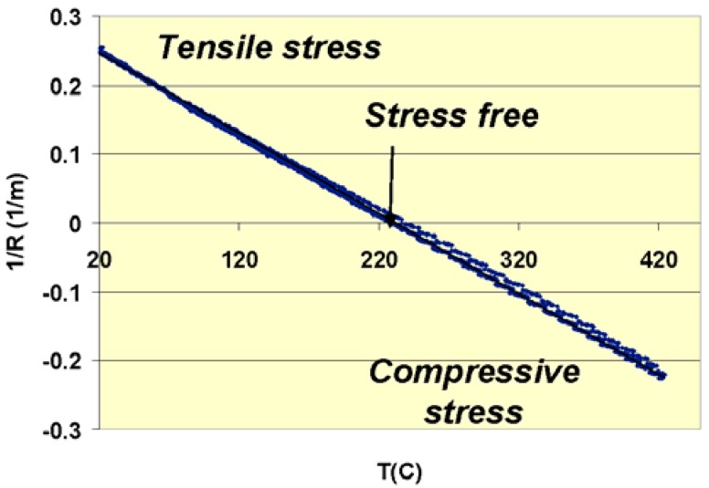
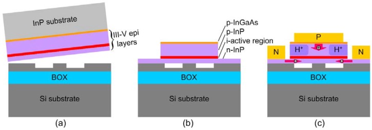
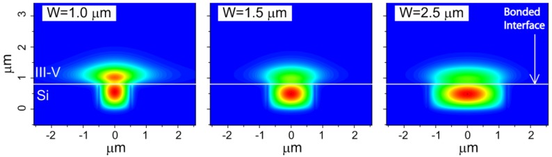
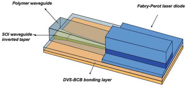
A review of recent progress in hybrid integrated platforms for silicon photonics is presented. Integration of III-V semiconductors onto silicon-on-insulator substrates based on two different bonding techniques is compared, one comprising only inorganic materials, the other technique using an organic bonding agent. Issues such as bonding process and mechanism, bonding strength, uniformity, wafer surface requirement, and stress distribution are studied in detail. The application in silicon photonics to realize high-performance active and passive photonic devices on low-cost silicon wafers is discussed. Hybrid integration is believed to be a promising technology in a variety of applications of silicon photonics.
Overview
The claims and statistics of this paper haven’t been checked yet.
Run the check — free, no account needed. It reads the open-access text and checks the sources it cites.
Integrity signals
Registry
Cites
Statistics
Figures
Verification
Claims the paper makes
The claims and statistics of this paper haven’t been checked yet.
Run the check — free, no account needed. It reads the open-access text and checks the sources it cites.
Claims other papers make about this one
Each is checked against this paper’s own text: does it say what the citing paper says it does?
The cited source says what the claim attributes to it.
In the citing paper
“Integration proximity of the (dissimilar) materials in direct bonding facilitates superior optical coupling and heat transportation between them56.”
From Roadmapping the next generation of silicon photonics (2024) · cites this paper as [56]
Self-check
Percentages, sums and reported differences re-computed from the paper’s own numbers.
The self-check needs the paper’s full text.
Citations
Cites
Device Requirements for Optical Interconnects to Silicon Chips
Miller, D. A. B. (2009) · Proceedings of the IEEE · doi:10.1109/jproc.2009.2014298 · Cited by 2,000
Electrically pumped hybrid AlGaInAs-silicon evanescent laser
Fang, A. W., Park, H., Cohen, O., Jones, R., Paniccia, M. J., & Bowers, J. E. (2006) · Optics Express · doi:10.1364/oe.14.009203 · Cited by 1,244
Self-citationBonding of silicon wafers for silicon-on-insulator
Maszara, W., Goetz, G., Caviglia, A. L., & McKitterick, J. B. (1988) · Journal of Applied Physics · doi:10.1063/1.342443 · Cited by 878
Gösele, U., & Tong, Q.-Y. (1998) · Annual Review of Materials Science · doi:10.1146/annurev.matsci.28.1.215 · Cited by 600
SemiConductor Wafer Bonding: Science and Technology
Tong, Q., & Gösele, U. (1998) · Cited by 555
Campenhout, J. V., Romeo, P. R., Régreny, P., Seassal, C., Thourhout, D. V., Verstuyft, S., Cioccio, L. D., Fédéli, J.-M., Lagahe, C., & Baets, R. (2007) · Optics Express · doi:10.1364/oe.15.006744 · Cited by 513
Self-citationNiklaus, F., Stemme, G., Lu, J., & Gutmann, R. J. (2006) · Journal of Applied Physics · doi:10.1063/1.2168512 · Cited by 473
Magneto-optical isolator with silicon waveguides fabricated by direct bonding
Shoji, Y., Mizumoto, T., Yokoi, H., Hsieh, I.-W., & Osgood, R. M. (2008) · Applied Physics Letters · doi:10.1063/1.2884855 · Cited by 336
Miller, D. A. B., & Özaktaş, H. M. (1997) · Journal of Parallel and Distributed Computing · doi:10.1006/jpdc.1996.1285 · Cited by 290
Plasma-assisted InP-to-Si low temperature wafer bonding
Pasquariello, D. M., & Hjort, K. (2002) · IEEE Journal of Selected Topics in Quantum Electronics · doi:10.1109/2944.991407 · Cited by 250
Cited by
Sorted by citations
Advances in quantum cryptography
Pirandola, S., Andersen, U. L., Banchi, L., Berta, M., Bunandar, D., Colbeck, R., Englund, D., Gehring, T., Lupo, C., Ottaviani, C., et al. (2020) · Advances in Optics and Photonics · doi:10.1364/aop.361502 · Cited by 2,033
Advances in Quantum Cryptography
Pirandola, S., Andersen, U. L., Banchi, L., Berta, M., Bunandar, D., Colbeck, R., Englund, D., Gehring, T., Lupo, C., Ottaviani, C., et al. (2019) · White Rose Research Online (University of Leeds, The University of Sheffield, University of York) · Cited by 1,566
Mid-infrared photonics in silicon and germanium
Soref, R. (2010) · Nature Photonics · doi:10.1038/nphoton.2010.171 · Cited by 1,460
Review of Silicon Photonics Technology and Platform Development
Siew, S. Y., Li, B., Gao, F., Zheng, H. Y., Zhang, W., Guo, P., Xie, S. W., Song, A., Dong, B., Luo, L. W., et al. (2021) · Journal of Lightwave Technology · doi:10.1109/jlt.2021.3066203 · Cited by 988
Roadmapping the next generation of silicon photonics
Shekhar, S., Bogaerts, W., Chrostowski, L., Bowers, J. E., Hochberg, M., Soref, R., & Shastri, B. J. (2024) · Nature Communications · doi:10.1038/s41467-024-44750-0 · Cited by 878
Self-citation
Metadata
- Authors
- Liang, D., Roelkens, G., Baets, R., & Bowers, J.
- Affiliations
- University of California, Santa Barbara (US)
- Photonics Research Group, IMEC - Ghent University, Sint-Pietersnieuwstraat 41, B-9000 Ghent, Belgium
- Ghent University (BE)
- Corresponding author
- Liang, Di
- Venue
- Materials
- Publisher
- MDPI AG
- Published
- 2010-03-12
- Volume
- 3
- Issue
- 3
- Pages
- 1782-1802
- ISSN
- 1996-1944 (ISSN-L)
- PMC
- PMC5445873
- OpenAlex
- W2112113449
- Cited by
- 316
- References
- 60
- Citations by year
- 2026: 6 · 2025: 19 · 2024: 17 · 2023: 20 · 2022: 27 · 2021: 21 · 2020: 18 · 2019: 15 · 2018: 27 · 2017: 23 · 2016: 26 · 2015: 28 · 2014: 25 · 2013: 19 · 2012: 14
- FWCI
- 11.10
- Type
- journal article
- Language
- en
- Open access
- gold
- doi.org
- Licence
- Locations
- Materials (publishedVersion, cc-by)
- Europe PMC (PubMed Central) (publishedVersion, cc-by)
- PubMed Central (publishedVersion, cc-by)
- Ghent University Academic Bibliography (Ghent University) (submittedVersion, other-oa)
- DOAJ (DOAJ: Directory of Open Access Journals) (submittedVersion)
- Funders
- Vlaamse regering
- Defense Advanced Research Projects Agency
- University of California, Santa Barbara
- Topics
- Physical Sciences › Engineering › Electrical and Electronic Engineering › Photonic and Optical Devices
- Physical Sciences › Engineering › Electrical and Electronic Engineering › 3D IC and TSV technologies
- Physical Sciences › Engineering › Electrical and Electronic Engineering › Semiconductor Lasers and Optical Devices
- Keywords
- hybrid integration, silicon photonics, III-V on silicon, silicon-on-insulator, wafer bonding, bond strength, stress distribution, active photonic devices, passive optical components
About these checks
Registry, retraction, Cites and statistics results are computed, not judged, with one exception: a printed reference that no index lists is read once by a model before it counts as a citation error. Claims are extracted by a model and kept only when their quote appears verbatim in the text; each cited source is then checked, with a model’s help, for whether it says what the claim relies on. Those verdicts can be wrong — read the claim’s quote and the cited source before relying on one.
Statistics and arithmetic are recomputed, not judged.
Confidence bands are shown only for fields calibrated on our annotated test set. None is calibrated yet, so no band is shown.
What counts as a claim ›How we measure confidence ›How we check this ›
Are you an author, or do you see a problem with this page? Request a review
