

Analytical modeling and doping optimization for enhanced analog performance in a Ge/Si interfaced nanowire MOSFET
Open accessThe DOI matches its Crossref record; 73 of the 74 references it cites were found in a registry or an index; none of the 24 sources its claims cite is checked for support yet.
Abstract
Doping of source, channel, and drain strongly affects nanowire MOSFET characteristics, and biosensing capability is also discussed.
Overview
CoChat Summary
TL;DR
This paper develops an analytical model and TCAD-based study of a Ge/Si interfaced nanowire MOSFET (GSI-NWM) to show how source, channel, and drain doping can be optimized for analog and biosensing performance. It reports substantial performance gains from doping optimization, including up to a 364 mV threshold-voltage reduction, ~10^6 times improvement in current ratio, and a 67.78 mV/decade subthreshold-swing reduction.
Key findings
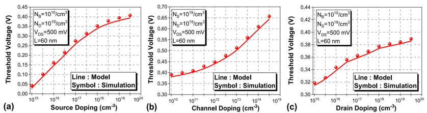
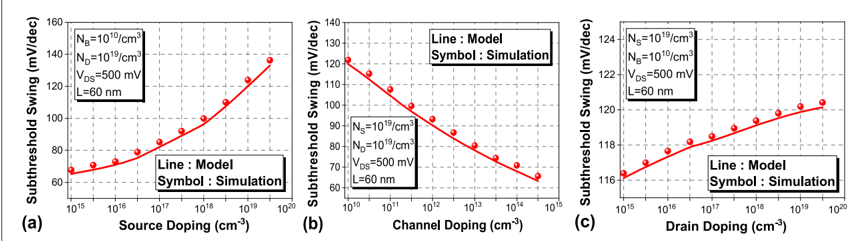
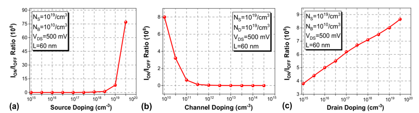
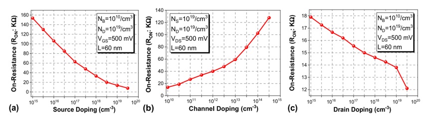
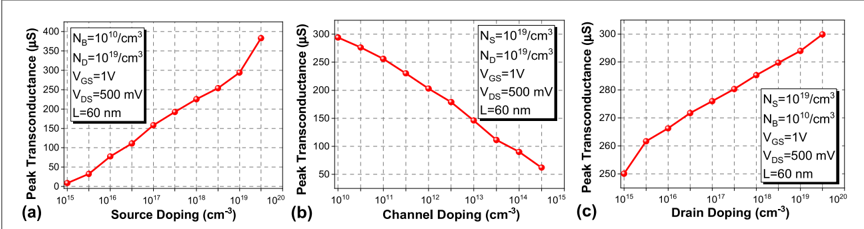
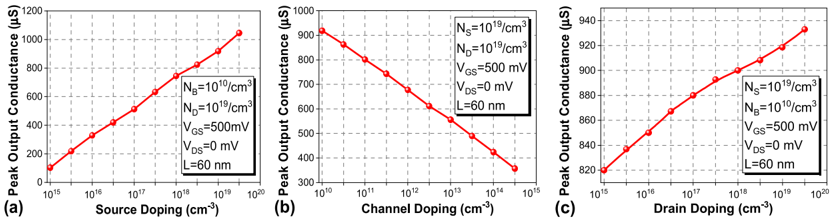
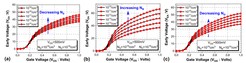
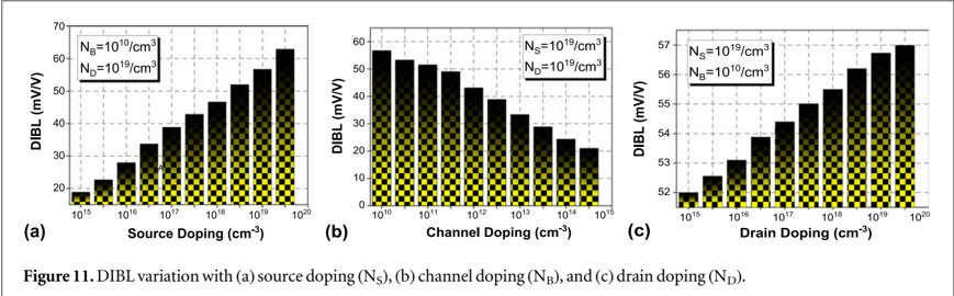
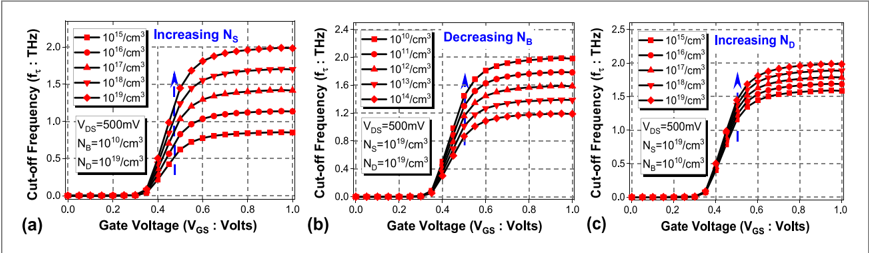
- Doping strongly changes the device’s analog behavior: source doping has the largest effect on most metrics, while channel doping most strongly affects early voltage and drain-induced barrier lowering; drain doping generally has a smaller effect than source/channel doping.
- The paper reports that doping optimization can achieve up to 364 mV reduction in threshold voltage, ~10^6 improvement in current ratio, 67.78 mV/decade reduction in subthreshold swing, and 145.81 kΩ reduction in on-resistance.
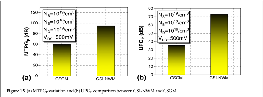
- Compared with a conventional surrounding-gate MOSFET (CSGM), the GSI-NWM shows much better reported figures in Table 6: off-current at \(V_{GS}=0\) V and \(V_{DS}=1\) V is 0.59 pA for GSI-NWM versus 29.18 pA for CSGM, and peak electric field near the drain is ~0.9405 × 10^6 V m^-1 versus ~1.288 × 10^6 V m^-1.
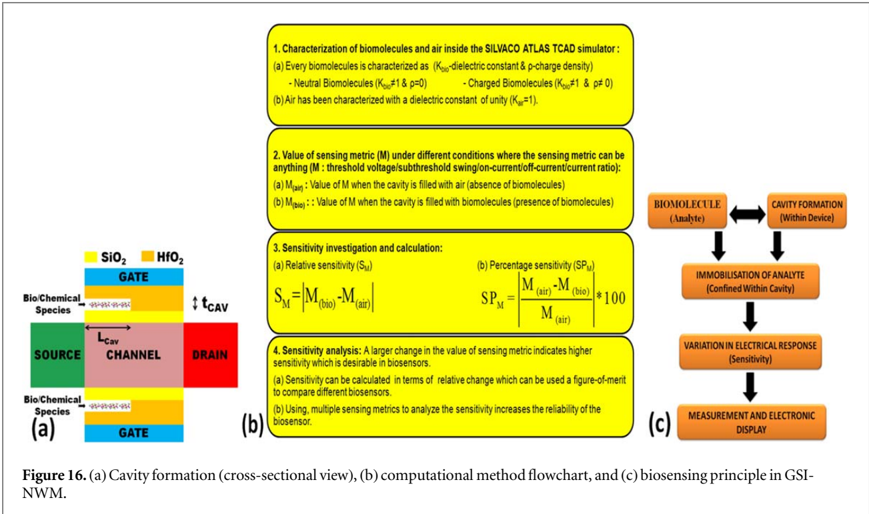
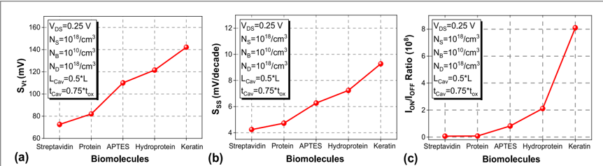
- For biosensing, higher biomolecule dielectric constant increases sensitivity; the paper states keratin (\(K_{bio}=8\)) gives the strongest response among the listed biomolecules, and Table 7 shows source-doping sensitivity for threshold voltage rising from 76.79 to 178.92 as doping increases from 10^16 to 10^19 cm^-3.
Methods
- The study combines a physics-based analytical model with DC and AC analysis in the SILVACO TCAD simulator.
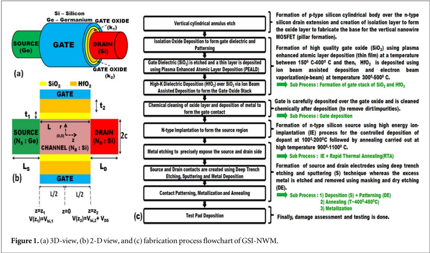
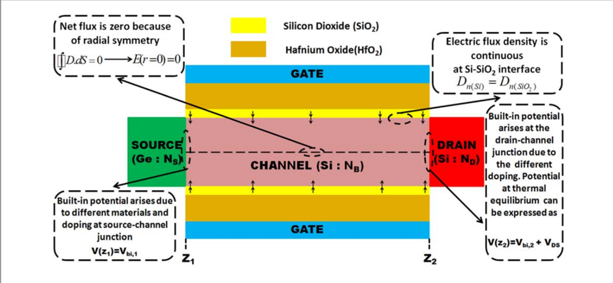
- The device studied is a Ge/Si interfaced nanowire MOSFET with 60 nm channel length and 20 nm channel thickness; the model uses Boltzmann statistics and a center-channel potential approach.
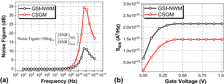
- Main analyses include threshold voltage, subthreshold swing, drain current, current ratio, on-resistance, transconductance, output conductance, early voltage, DIBL, cut-off frequency, transconductance frequency product, noise figure, S-parameters, and a biosensing cavity model.
Limitations
- The paper states it does not take into account ballistic transport and quantum mechanical effects, noting these become dominant only when channel length and thickness are less than 10 nm.
- Evident from the text: the conclusions are based on analytical modeling and simulation, and the paper does not report experimental fabrication or measurement of the proposed device.
- Evident from the text: several results are framed as comparisons to a CSGM with selected matched parameters, so the scope is limited to the modeled structures and conditions described in the paper.
Model-written summary. Check it against the paper before relying on it.
Integrity signals
Registry
Cites
Statistics
Figures
Verification
Claims the paper makes
0 Valid · 3 Not valid · 17 Not checked · 70 Own results and interpretations
A result the paper reports from its own data — it cites no other source for it, so there is none to check. The quote shows it is in the paper.
In the paper
“The doping of source, channel, and drain has a prominent effect on important device characteristics, which has been investigated through DC and AC analysis performed on the SILVACO TCAD simulator.”
§ Analytical modeling and doping optimization for enhanced analog performance in a Ge/Si interfaced nanowire MOSFET > Abstract
boostedstates a cause- Asserted: passes — The authors put it forward as true.
- Checkable: passes — It can be checked against evidence.
- Load-bearing: passes — The paper’s conclusions depend on it.
- Based: passes — The paper gives a reason why it holds.
A result the paper reports from its own data — it cites no other source for it, so there is none to check. The quote shows it is in the paper.
In the paper
“The investigation revealed a strong dependence of most of these characteristics on the source, channel, and drain doping levels, providing valuable insights into device performance.”
§ Analytical modeling and doping optimization for enhanced analog performance in a Ge/Si interfaced nanowire MOSFET > Abstract
boostedstates an association- Asserted: passes — The authors put it forward as true.
- Checkable: passes — It can be checked against evidence.
- Load-bearing: passes — The paper’s conclusions depend on it.
- Based: passes — The paper gives a reason why it holds.
A result the paper reports from its own data — it cites no other source for it, so there is none to check. The quote shows it is in the paper.
In the paper
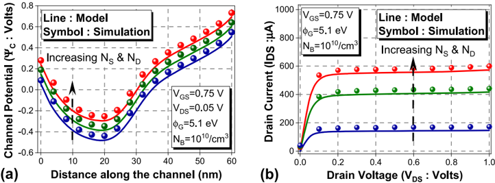
“A compact physics-based analytical model has been mathematically evaluated and proposed in this work, showing an excellent in-line agreement with the simulated results.”
§ Analytical modeling and doping optimization for enhanced analog performance in a Ge/Si interfaced nanowire MOSFET > Abstract
boostedstates an association- Asserted: passes — The authors put it forward as true.
- Checkable: passes — It can be checked against evidence.
- Load-bearing: passes — The paper’s conclusions depend on it.
- Based: passes — The paper gives a reason why it holds.
A result the paper states — it cites no source for it, so there is none to check. The quote shows it is in the paper.
In the paper
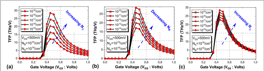
“The swing in the current decreases (due to a reduction in both on-current and offcurrent) with the increasing N B, whereas the swing increases slightly with the increasing N D .”
§ Analytical modeling and doping optimization for enhanced analog performance in a Ge/Si interfaced nanowire MOSFET > 4.1. Effect of doping on analog performance evaluation characteristics
plainstates a cause- Asserted: passes — The authors put it forward as true.
- Checkable: passes — It can be checked against evidence.
- Load-bearing: passes — The paper’s conclusions depend on it.
- Based: passes — The paper gives a reason why it holds.
A result the paper states — it cites no source for it, so there is none to check. The quote shows it is in the paper.
In the paper
“Most of the depletion region across the drain junction will deeply penetrate inside the channel at high drain doping, which increases the CLM, and hence, V EA increases with the increasing N D .”
§ Analytical modeling and doping optimization for enhanced analog performance in a Ge/Si interfaced nanowire MOSFET > But, the I ON /I
plainstates a cause- Asserted: passes — The authors put it forward as true.
- Checkable: passes — It can be checked against evidence.
- Load-bearing: passes — The paper’s conclusions depend on it.
- Based: passes — The paper gives a reason why it holds.
53 more claims
Create a free account to see all 90 claims and to verify the 1 reference still open.
- It may state two separate claims as one. 20
- Probably not a substantial claim. 13
Citations
Cites
Essential physics of carrier transport in nanoscale MOSFETs
Lundstrom, M., & Ren, Z. (2002) · IEEE Transactions on Electron Devices · doi:10.1109/16.974760 · Cited by 554
Review on high-k dielectrics reliability issues
Ribes, G., Mitard, J., Denais, M., Bruyere, S., Monsieur, F., Parthasarathy, C., Vincent, E., & Ghibaudo, G. (2005) · IEEE Transactions on Device and Materials Reliability · doi:10.1109/tdmr.2005.845236 · Cited by 533
Brunco, D. P., De Jaeger, B., Eneman, G., Mitard, J., Hellings, G., Satta, A., Terzieva, V., Souriau, L., Leys, F. E., Pourtois, G., et al. (2008) · Journal of The Electrochemical Society · doi:10.1149/1.2919115 · Cited by 267
Madan, J., & Chaujar, R. (2016) · IEEE Transactions on Device and Materials Reliability · doi:10.1109/tdmr.2016.2564448 · Cited by 231
Zamzami, M. A., Rabbani, G., Ahmad, A., Basalah, A. A., Al-Sabban, W. H., Nate Ahn, S., & Choudhry, H. (2022) · Bioelectrochemistry · doi:10.1016/j.bioelechem.2021.107982 · Cited by 211
Ajay, Narang, R., Saxena, M., & Gupta, M. (2017) · IEEE Sensors Journal · doi:10.1109/jsen.2017.2716102 · Cited by 114
Investigation of a Ge-Source Vertical TFET With Delta-Doped Layer
Vanlalawmpuia, K., & Bhowmick, B. (2019) · IEEE Transactions on Electron Devices · doi:10.1109/ted.2019.2933313 · Cited by 104
Pratap, Y., Kumar, M., Kabra, S., Haldar, S., Gupta, R. S., & Gupta, M. (2018) · Journal of Computational Electronics · doi:10.1007/s10825-017-1041-4 · Cited by 99
Self-citationChakraborty, A., & Sarkar, A. (2017) · Journal of Computational Electronics · doi:10.1007/s10825-017-0999-2 · Cited by 94
Kranti, A., Haldar, S., & Gupta, R. S. (2001) · Microelectronic Engineering · doi:10.1016/s0167-9317(00)00419-6 · Cited by 90
Self-citationKumar, M., Subhasis Haldar, C., Gupta, M., & Gupta, R. (2014) · Microelectronics Journal · doi:10.1016/j.mejo.2014.07.010 · Cited by 88
Self-citationDas, A., Rewari, S., Kanaujia, B. K., & Gupta, R. (2021) · Silicon · doi:10.1007/s12633-021-01288-w · Cited by 84
Self-citationAnalysis of Short-Channel Effects in Junctionless DG MOSFETs
(2017) · doi:10.1109/ted.2017.2716969 · Cited by 73
Dielectric modulated junctionless biotube FET (DM-JL-BT-FET) Bio-Sensor
Goel, A., Rewari, S., Verma, S., Deswal, S. S., & Gupta, R. S. (2021) · IEEE Sensors Journal · doi:10.1109/jsen.2021.3077540 · Cited by 69 · cited 1×
“57) [34], hydroprotein (Kbio= 5) [70] or keratin (Kbio= 8) [71] are entrapped inside the cavity, thefield and potential changes due to the change in oxide capacitance.”
BackgroundSelf-citationA Review of Carbon Nanotubes Field Effect-Based Biosensors
Alabsi, S. S., Ahmed, A. Y., Dennis, J. O., Khir, M. H. M., & Algamili, A. S. (2020) · IEEE Access · doi:10.1109/access.2020.2987204 · Cited by 68
Das, A., Rewari, S., Kanaujia, B. K., Deswal, S. S., & Gupta, R. S. (2023) · Journal of Computational Electronics · doi:10.1007/s10825-023-02008-w · Cited by 67
Self-citationGe/Si interfaced label free nanowire BIOFET for biomolecules detection - analytical analysis
Das, A., Rewari, S., Kanaujia, B. K., Deswal, S. S., & Gupta, R. (2023) · Microelectronics Journal · doi:10.1016/j.mejo.2023.105832 · Cited by 61
Self-citationDas, A., Kanaujia, B. K., Nath, V., Rewari, S., & Gupta, R. (2020) · IEEE India Conference · doi:10.1109/indicon49873.2020.9342175 · Cited by 58
Self-citationDas, R., Chanda, M., & Sarkar, C. K. (2018) · IEEE Transactions on Electron Devices · doi:10.1109/ted.2018.2872466 · Cited by 57
Gautam, R., Saxena, M., Gupta, R. S., & Gupta, M. (2013) · IEEE Transactions on Electron Devices · doi:10.1109/ted.2013.2256912 · Cited by 55
Self-citationDas, A., Rewari, S., Kanaujia, B. K., Deswal, S. S., & Gupta, R. (2023) · International Journal of Numerical Modelling Electronic Networks Devices and Fields · doi:10.1002/jnm.3106 · Cited by 54
Self-citationEssential physics of carrier transport in nanoscale MOSFETs
Lundstrom, M., Ren, Z., & Datta, S. (2002) · International Conference on Simulation of Semiconductor Processes and Devices · doi:10.1109/sispad.2000.871193 · Cited by 54
Tamersit, K., & Djeffal, F. (2019) · IEEE Sensors Journal · doi:10.1109/jsen.2019.2925597 · Cited by 49
Modeling of gate underlap junctionless double gate MOSFET as bio-sensor
Ajay, Narang, R., Saxena, M. K., & Gupta, M. (2017) · Materials Science in Semiconductor Processing · doi:10.1016/j.mssp.2017.08.008 · Cited by 49
Two-dimensional quantum effects in nanoscale MOSFETs
(2002) · doi:10.1109/16.974744 · Cited by 48
Rewari, S., Nath, V., Subhasis Haldar, C., Deswal, S. S., & Gupta, R. (2017) · Microsystem Technologies · doi:10.1007/s00542-017-3436-3 · Cited by 41
Self-citationFerhati, H., Djeffal, F., & Bentrcia, T. (2018) · Beilstein Journal of Nanotechnology · doi:10.3762/bjnano.9.177 · Cited by 41
A review of carbon-based materials and their coating techniques for biomedical implants applications
Hassan, S., Nadeem, A. Y., Qaiser, H., Kashif, A. S., Ahmed, A., Khan, K., & Altaf, A. (2023) · Carbon letters · doi:10.1007/s42823-023-00496-1 · Cited by 40
Pradhan, K. P., Kumar, M., Mohapatra, S. K., & Sahu, P. K. (2015) · Ain Shams Engineering Journal · doi:10.1016/j.asej.2015.04.009 · Cited by 38
Patil, G. C., & Qureshi, S. (2011) · Semiconductor Science and Technology · doi:10.1088/0268-1242/26/8/085002 · Cited by 37
Das, A., Kanaujia, B. K., Deswal, S. S., Rewari, S., & Gupta, R. (2022) · IEEE International Conference of Electron Devices Society Kolkata Chapter (EDKCON) · doi:10.1109/edkcon56221.2022.10032940 · Cited by 34
Self-citationImpact of nanowire variability on performance and reliability of gate-all-around III-V MOSFETs
Shin, S. H., Masuduzzaman, M., Gu, J. J., Wahab, M. A., Conrad, N., Si, M., Ye, P. D., & Alam, M. A. (2013) · 2013 IEEE International Electron Devices Meeting · doi:10.1109/iedm.2013.6724582 · Cited by 34
Singh, A. K., Tripathy, M. R., Baral, K., Singh, P. K., & Jit, S. (2020) · Applied Physics A · doi:10.1007/s00339-020-03869-9 · Cited by 33
Wu, H., Si, M., Dong, L., Gu, J., Zhang, J., & Ye, P. D. (2015) · IEEE Transactions on Electron Devices · doi:10.1109/ted.2015.2412878 · Cited by 32
(2020) · doi:10.1007/s11664-020-08541-9 · Cited by 32
Self-citationSharma, S., Nath, V., Deswal, S. S., & Gupta, R. S. (2022) · Microelectronics Journal · doi:10.1016/j.mejo.2022.105599 · Cited by 31
Self-citationA novel double gate MOSFET by symmetrical insulator packets with improved short channel effects
Ramezani, Z., & Orouji, A. A. (2017) · International Journal of Electronics · doi:10.1080/00207217.2017.1357206 · Cited by 31
Ganesh, A., Goel, K., Mayall, J. S., & Rewari, S. (2021) · Silicon · doi:10.1007/s12633-021-01173-6 · Cited by 28
Self-citationDielectric modulated triple metal gate all around MOSFET (TMGAA)for DNA bio-molecule detection
Goel, A., Rewari, S., Verma, S., & Gupta, R. S. (2018) · 2018 IEEE Electron Devices Kolkata Conference (EDKCON) · doi:10.1109/edkcon.2018.8770406 · Cited by 27
Self-citationYirak, M. G., & Chaujar, R. (2022) · Journal of Electronic Materials · doi:10.1007/s11664-022-09466-1 · Cited by 26
Cherik, I. C., Mohammadi, S., & Orouji, A. A. (2022) · IEEE Transactions on Electron Devices · doi:10.1109/ted.2021.3124984 · Cited by 23
Exploring the Effect of Device Aging on Static Power Analysis Attacks
Karimi, N., Moos, T., & Moradi, A. (2019) · IACR Trans. Cryptogr. Hardw. Embed. Syst. · doi:10.13154/tches.v2019.i3.233-256 · Cited by 23
Exploring the Effect of Device Aging on Static Power Analysis Attacks
Karimi, N., Moos, T., & Moradi, A. (2019) · IACR Transactions on Cryptographic Hardware and Embedded Systems · doi:10.46586/tches.v2019.i3.233-256 · Cited by 20
Source material valuation of charge plasma based DG-TFET for RFIC applications
(2022) · doi:10.1088/1361-6641/ac7ede · Cited by 18
Self-citationVenkatesh, M., Priya, G. L., & Balamurugan, N. B. (2021) · Silicon · doi:10.1007/s12633-020-00856-w · Cited by 16
Maiti, S., De, A., & Sarkar, S. K. (2021) · Silicon · doi:10.1007/s12633-021-01415-7 · Cited by 15
Sharma, S., Goel, A., Rewari, S., Nath, V., & Gupta, R. (2022) · Silicon · doi:10.1007/s12633-022-01663-1 · Cited by 14
Self-citationGoyal, P., & Kaur, H. (2022) · Micro and Nanostructures · doi:10.1016/j.micrna.2022.207454 · Cited by 9
Kumar, M., Haldar, S., Gupta, M., & Gupta, R. S. (2017) · Superlattices and Microstructures · doi:10.1016/j.spmi.2017.04.034 · Cited by 9
Self-citationL-Shaped Schottky Barrier MOSFET for High Performance Analog and RF Applications
Rashid, S., Bashir, F., Khanday, F. A., & Beigh, M. R. (2023) · Silicon · doi:10.1007/s12633-022-02006-w · Cited by 7
Solution Processable Nanowire Field-Effect Transistors
Opoku, C., Chen, L., Meyer, F., & Shkunov, M. (2011) · MRS Proceedings · doi:10.1557/opl.2011.1437 · Cited by 7
Jaiswal, S., & Gupta, S. K. (2022) · Silicon · doi:10.1007/s12633-022-02269-3 · Cited by 7
Saha, P., & Dhar, R. S. (2022) · International Journal of Nanoparticles · doi:10.1504/ijnp.2022.126376 · Cited by 1
Quantum mechanical effects on the threshold voltage of the evenly doped surrounding-gate MOSFETs
Mei, G., Li, P., Hu, G., et al. (2011) · 2011 9th IEEE International Conference on ASIC · doi:10.1109/asicon.2011.6157265
Mishra, V., Verma, Y. K., Gupta, S. K., et al. (2021) · doi:10.21203/rs.3.rs-229785/v1
Ganesh, A., Goel, K., Mayall, J. S., & Rewari, S. (2021) · doi:10.21203/rs.3.rs-360819/v1
Self-citation
Research works printed but not linked: 3
- 40. Sze S M 2017 VLSI Technology (McGraw Hill Education)
- 51. Software D S 2018 ATLAS User's Manual Device Simulation Software I 318
- 52. Adel S S and Smith K C 2020 Microelectronics Circuit (Oxford)
Cited by
Yadav, S., Das, A., & Rewari, S. (2024) · ECS Journal of Solid State Science and Technology · doi:10.1149/2162-8777/ad3364 · Cited by 65
Self-citationDas, A., Rewari, S., Kanaujia, B. K., Deswal, S. S., & Gupta, R. S. (2023) · Physica Scripta · doi:10.1088/1402-4896/acf4c9 · Cited by 62
Self-citationDas, A., Rewari, S., Kanaujia, B. K., Deswal, S. S., & Gupta, R. (2025) · Micro and Nanostructures · doi:10.1016/j.micrna.2025.208152 · Cited by 38
Self-citationKumar, V., Alam, M. N., & Park, S. (2024) · Polymer Composites · doi:10.1002/pc.28664 · Cited by 29
Kaul, A., Yadav, S., Rewari, S., & Nand, D. (2024) · Micro and Nanostructures · doi:10.1016/j.micrna.2024.207851 · Cited by 32
Self-citation
Metadata
- Authors
- Das, A., Rewari, S., Kanaujia, B. K., Deswal, S. S., & Gupta, R. S.
- Affiliations
- Jawaharlal Nehru University (IN)
- Delhi Technological University (IN)
- Corresponding author
- Das, Amit
- Venue
- Physica Scripta
- Publisher
- IOP Publishing
- Published
- 2023-06-27
- Volume
- 98
- Issue
- 7
- Pages
- 074005
- ISSN
- 0031-8949 (ISSN-L)
- 1402-4896
- OpenAlex
- W4380446660
- Cited by
- 49
- References
- 74
- Citations by year
- 2026: 4 · 2025: 21 · 2024: 17 · 2023: 7
- FWCI
- 3.64
- Type
- journal article
- Language
- en
- Open access
- bronze
- doi.org
- Licence
- publishingsupport.iopscience.iop.org/iop-standard/v1 (vor)
- iopscience.iop.org/info/page/text-and-data-mining (tdm)
- Locations
- Physica Scripta (publishedVersion)
- Topics
- Physical Sciences › Engineering › Electrical and Electronic Engineering › Advancements in Semiconductor Devices and Circuit Design
- Physical Sciences › Materials Science › Electronic, Optical and Magnetic Materials › Nanowire Synthesis and Applications
- Physical Sciences › Engineering › Electrical and Electronic Engineering › Semiconductor materials and devices
- Keywords
- doping optimization, analog performance, threshold voltage, cutoff frequency, subthreshold swing, transconductance, channel resistance, compact analytical model, biosensing
About these checks
Registry, retraction, Cites and statistics results are computed, not judged, with one exception: a printed reference that no index lists is read once by a model before it counts as a citation error. Claims are extracted by a model and kept only when their quote appears verbatim in the text; each cited source is then checked, with a model’s help, for whether it says what the claim relies on. Those verdicts can be wrong — read the claim’s quote and the cited source before relying on one.
A language model drew the claims from the paper on 2026-10-10, under version 3 of the claim definition (model deepseek-v4.1-flash, prompt extract-v3).
A second model labelled each claim on 2026-10-10 (model jev-1.13-20260917, definition revision gold-guideline-v0.2).
Statistics and arithmetic are recomputed, not judged.
Confidence bands are shown only for fields calibrated on our annotated test set. None is calibrated yet, so no band is shown.
What counts as a claim ›How we measure confidence ›How we check this ›
Are you an author, or do you see a problem with this page? Request a review
Data sources
Bibliographic data: Semantic Scholar, OpenAlex, Crossref.
Contains information from the Semantic Scholar Academic Graph Datasets, made available under the ODC Attribution License (ODC-BY 1.0).
Semantic Scholar’s data is described in: Kinney, R., et al. (2023). The Semantic Scholar Open Data Platform. arXiv:2301.10140.
