

Nonlinear integrated quantum electro-optic circuits
Open accessThe DOI matches its Crossref record; 34 of the 34 references it cites were found in a registry or an index; 2 of the 9 sources its claims cite were checked for support.
Abstract
An integrated chip with quantum state generation, active polarization manipulation, and precise time control is demonstrated.
Overview
CoChat Summary
TL;DR
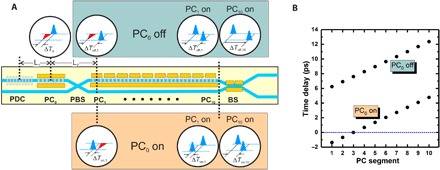
The paper demonstrates a monolithic Ti:LiNbO₃ electro-optic quantum circuit that integrates photon-pair generation, polarization routing/rotation, electro-optic switching, and adjustable on-chip time delay for Hong-Ou-Mandel interference. It reports on-chip HOM interference with 93.5 ± 1.8% visibility and programmable delays from ~1.3 ps to more than 12 ps.
Key findings
- A single Ti:LiNbO₃ chip generated degenerate telecom photon pairs via type II quasi-phase-matched PDC, separated them with an integrated PBS, actively rotated polarization with electro-optic PCs, and recombined them at a voltage-tunable balanced BS.
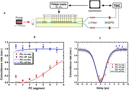
- On-chip HOM interference was observed with visibility 93.5 ± 1.8% at a pump power of ~100 μW, significantly above the 50% classical limit.
- The birefringent electro-optic delay (BED) line provided a relative time delay variable from ~1.3 ps to more than 12 ps, with discrete steps and resolution down to ~0.6 ps; 16 delays were designed, but only 14 were possible experimentally because the PC10 electrode was broken.
- The measured HOM dip temporal width was around 5.5 ps, and the device had total loss around 11 dB, corresponding to a Klyshko efficiency of 5%; PDC brightness was estimated at ~3 × 10⁵ pairs/(s·mW·nm).
Methods
- The circuit was fabricated on z-cut LiNbO₃ by Ti indiffusion, with periodically poled PDC and PC sections, SiO₂ buffer, patterned Al electrodes, AR/HR coatings, and temperature-stabilized mounting.
- Component lengths included a 20.7-mm PDC section (Λ_PDC = 9.04 μm), 7.62-mm PC0, 4.0-mm PBS, 10 segmented PC elements of 2.54 mm each, and a 13.1-mm BS; overall structure length was slightly more than 70 mm.
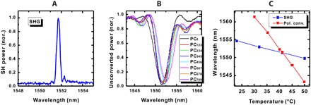
- Classical characterization used SHG, broadband spectral transmission, and temperature dependence to set the operating point at T = 43.6°C and λ = 1551.7 nm; quantum measurements used a ~776-nm pump, fiber filters, SNSPDs, and a TDC, with unitary-transformation simulations for comparison.
Limitations
- Stated: the discrete on-chip time delay prevented resolving the real shape of the HOM dip, and only seven triples of the segmented PC could be addressed because the PC10 electrode was broken, allowing only 14 different delays.
- Stated: simulations ignored the slight spectral shift of different PCs and the consequent spectral mismatch among PDC photons and fiber filters; incomplete conversion of PC0 strongly affected the HOM dip and could produce fast oscillations not resolvable with the current discrete delay resolution.
- Evident from the text: the demonstration is limited to one Ti:LiNbO₃ device and does not measure the full HOM dip; non-unity visibility is attributed to accumulated imperfections from individual components.
Model-written summary. Check it against the paper before relying on it.
Integrity signals
Registry
Cites
Statistics
Figures

Verification
Claims the paper makes
2 Valid · 5 Not valid · 6 Not checked · 43 Own results and interpretations
Every source the paper cites for this claim was checked and supports it.
In the paper
“After PC0, the H- and V-polarized photons are spatially separated at the PBS (29).”
§ Nonlinear integrated quantum electro-optic circuits > RESULTS > Birefringent electro-optic delay
What the sources say
- Supportedcites [29] Sansoni L., Luo K. H., Eigner C., Ricken R., Quiring V., Herrmann H., Silberhorn C., A two-channel, spectrally degenerate polarization entangled source on chip. NPJ Quant. Inf. 3, 5 (2017). source
The attributed content — that a PBS sends the H- and V-polarized photons into different spatial outputs — is stated repeatedly in our copy: the RESULTS (p. 1) describe type II pairs 'split on an integrated polarizing beam splitter (PBS)' giving |HA,VB〉 / |VA,HB〉, and RESULTS (p. 2) formalize the PBS input-to-output mode transformation with transmissivity/reflected amplitudes; MATERIALS AND METHODS (p. 3) give measured transmission for H and reflectivity for V (T_H = 0.996 ± 0.002, R_V = 0.968 ± 0.003), and the abstract/DISCUSSION (pp. 1, 3) stress emission of entangled photons 'into different spatial modes'. The 'PC0' element is a component of the citing authors' own apparatus and does not appear in this source (its setup uses a Sagnac loop, waveplates, LCD, PMFs and FBGs, Materials and Methods pp. 3-4); it is not part of what the citation asserts, so it does not weaken the verdict. (LLM, conf=0.85)
plainstates a cause- Asserted: passes — The authors put it forward as true.
- Checkable: passes — It can be checked against evidence.
- Load-bearing: passes — The paper’s conclusions depend on it.
- Based: passes — The paper gives a reason why it holds.
- Supported
Every source the paper cites for this claim was checked and supports it.
In the paper
“For example, when PC0 only converts half of the polarization, hyperentanglement can be generated if the design parameters are carefully chosen (32).”
§ Nonlinear integrated quantum electro-optic circuits > DISCUSSION
What the sources say
- Supportedcites [32] Sharapova P. R., Luo K. H., Herrmann H., Reichelt M., Silberhorn C., Meier T., Modified two-photon interference achieved by the manipulation of entanglement. Phys. Rev. A 96, 043857 (2017). source
The paper calls the converter PC1 rather than PC0. It states that a π/4 rotation puts the photons in equal-amplitude polarization superpositions (p. 3), and that, with an appropriate channel length, the resulting spatial entanglement combines with preserved frequency entanglement to create hyperentanglement (pp. 3–4). (LLM, conf=0.90)
plainstates a possible cause- Asserted: passes — The authors put it forward as true.
- Checkable: passes — It can be checked against evidence.
- Load-bearing: unclear — It is unclear whether the paper’s conclusions depend on it.
- Based: passes — The paper gives a reason why it holds.
- Supported
A result the paper reports from its own data — it cites no other source for it, so there is none to check. The quote shows it is in the paper.
In the paper
“With the configuration of the present device, we can vary the relative time delay between ~1.3 ps and more than 12 ps, as shown in Fig. 2B.”
§ Nonlinear integrated quantum electro-optic circuits > RESULTS > Birefringent electro-optic delay
plain- Asserted: passes — The authors put it forward as true.
- Checkable: passes — It can be checked against evidence.
- Load-bearing: passes — The paper’s conclusions depend on it.
- Based: passes — The paper gives a reason why it holds.
In the paper
“Our monolithic solution is realized on the Ti:LiNbO3 platform (26), which exploits the strong χ(2) nonlinearity for both photon pair generation and electro-optic manipulation of the qubits.”
§ Nonlinear integrated quantum electro-optic circuits > RESULTS
What the sources say
- Not checked yetcites [26] K.-H. Luo, S. Brauner, C. Eigner, P. R. Sharapova, R. Ricken, T. Meier, H. Herrmann, C. Silberhorn, Monolithically integrated Hong-Ou-Mandel experiment in LiNbO3, in Conference on Lasers and Electro-Optics, OSA Terchnical Digest (online) (Optical Society of America, 2018), paper FM1G.3. source
boostedstates a cause- Asserted: passes — The authors put it forward as true.
- Checkable: passes — It can be checked against evidence.
- Load-bearing: passes — The paper’s conclusions depend on it.
- Based: passes — The paper gives a reason why it holds.
A result the paper reports from its own data — it cites no other source for it, so there is none to check. The quote shows it is in the paper.
In the paper
“Although the central wavelengths are slightly different, which we attribute to inhomogeneities in the fabrication process, all conversion bands overlap reasonably well.”
§ Nonlinear integrated quantum electro-optic circuits > RESULTS > Experimental characterization
plain- Asserted: passes — The authors put it forward as true.
- Checkable: passes — It can be checked against evidence.
- Load-bearing: passes — The paper’s conclusions depend on it.
- Based: passes — The paper gives a reason why it holds.
18 more claims
Create a free account to see all 56 claims and to verify the 7 references still open.
- It may state two separate claims as one. 24
- Probably not a substantial claim. 12
Claims other papers make about this one
Each is checked against this paper’s own text: does it say what the citing paper says it does?
The cited source says what the claim attributes to it.
In the citing paper
“LN will possibly be a valuable material for future photonic chips at is has a strong χ (2) nonlinearity and can be used to provide precise timing control via EO modulation [238].”
From 2022 Roadmap on integrated quantum photonics (2022) · cites this paper as [238]
Self-check
Percentages, sums and reported differences re-computed from the paper’s own numbers.
Each contradiction between two passages listed here was confirmed by an independent check.
Rated minor: it would not touch a result — a value no result rests on, a p-value that stays on the same side of the significance level, or a conflict that is clerical, resolved elsewhere in the paper, or outside its own findings.
In the paper
§ Nonlinear integrated quantum electro-optic circuits > RESULTS
“The H-polarized photons leave the splitter at the bar-state output, and V photons leave the splitter at the cross-state output.”
§ Nonlinear integrated quantum electro-optic circuits > MATERIALS AND METHODS > Components and circuit design
“routing of the H-polarized photons to the cross-state output of the coupler, whereas the V-polarized photons are directed into the bar-state output.”
Citations
Cites
A scheme for efficient quantum computation with linear optics
Knill, E., Laflamme, R., & Milburn, G. J. (2001) · Nature · doi:10.1038/35051009 · Cited by 5,880 · cited 1×
“For example, boson sampling [4, 5], Bell-state measurement for quantum repeaters, and KLM protocol for quantum computing [25] rely on HOM interference.”
MethodMeasurement of subpicosecond time intervals between two photons by interference
Hong, C. K., Ou, Z. Y., & Mandel, L. (1987) · Physical Review Letters · doi:10.1103/physrevlett.59.2044 · Cited by 4,369 · cited 2×
“[22] C.”
MethodGiovannetti, V., Lloyd, S., & Maccone, L. (2011) · Nature Photonics · doi:10.1038/nphoton.2011.35 · Cited by 3,894 · cited 1×
“In the past decade, many optical circuits for quantum gates [1], quantum interference [2], quantum metrology [3], boson sampling [4, 5] and quantum walks [6, 7] in different materials have been demonstrated.”
BackgroundNew CMOS-compatible platforms based on silicon nitride and Hydex for nonlinear optics
Moss, D. J., Morandotti, R., Gaeta, A. L., & Lipson, M. (2013) · Nature Photonics · doi:10.1038/nphoton.2013.183 · Cited by 1,792 · cited 1×
“Most of these circuits are realized in materials with χ((3)) nonlinearities like glass [8, 9], silicon nitride [10], silicon-on insulator [11] and silica-on-silicon [12– 15].”
BackgroundA review of lithium niobate modulators for fiber-optic communications systems
Wooten, E. L., Kissa, K. M., Yi-Yan, A., Murphy, E. J., Lafaw, D. A., Hallemeier, P. F., Maack, D., Attanasio, D. V., Fritz, D. J., McBrien, G. J., et al. (2000) · IEEE Journal of Selected Topics in Quantum Electronics · doi:10.1109/2944.826874 · Cited by 1,330
Carolan, J., Harrold, C., Sparrow, C., Martín-López, E., Russell, N. J., Silverstone, J. W., Shadbolt, P. J., Matsuda, N., Oguma, M., Itoh, M., et al. (2015) · Science · doi:10.1126/science.aab3642 · Cited by 1,093
Silica-on-silicon waveguide quantum circuits
Politi, A., Cryan, M. J., Rarity, J. G., Yu, S., & O'Brien, J. L. (2008) · Science · doi:10.1126/science.1155441 · Cited by 1,084
Quantum Walks of Correlated Photons
Peruzzo, A., Lobino, M., Matthews, J. C. F., Matsuda, N., Politi, A., Poulios, K., Zhou, X.-Q., Lahini, Y., Ismail, N., Wörhoff, K., et al. (2010) · Science · doi:10.1126/science.1193515 · Cited by 929
Boson Sampling on a Photonic Chip
Spring, J. B., Metcalf, B. J., Humphreys, P. C., Kolthammer, W. S., Jin, X.-M., Barbieri, M., Datta, A., Thomas-Peter, N., Langford, N. K., Kundys, D., et al. (2013) · Science · doi:10.1126/science.1231692 · Cited by 837
Tillmann, M., Dakić, B., Heilmann, R., Nolte, S., Szameit, A., & Walther, P. (2013) · Nature Photonics · doi:10.1038/nphoton.2013.102 · Cited by 709
Photonic Boson Sampling in a Tunable Circuit
Broome, M. A., Fedrizzi, A., Rahimi-Keshari, S., Dove, J., Aaronson, S., Ralph, T. C., & White, A. G. (2013) · Science · doi:10.1126/science.1231440 · Cited by 634
All-photonic quantum repeaters
Azuma, K., Tamaki, K., & Lo, H.-K. (2015) · Nature Communications · doi:10.1038/ncomms7787 · Cited by 583 · cited 1×
“As one of the most fundamental nonclassical experiments in quantum optics, it lies at the heart of many quantum logic operations (23), for example, boson sampling (6, 7); Bell-state measurement for quantum repeaters (24); and the Knill, Laflamme, and Milburn protocol for quantum computing (25).”
BackgroundOn-chip quantum interference between silicon photon-pair sources
Silverstone, J. W., Bonneau, D., Ohira, K., Suzuki, N., Yoshida, H., Iizuka, N., Ezaki, M., Natarajan, C. M., Tanner, M. G., Hadfield, R. H., et al. (2014) · Nature Photonics · doi:10.1038/nphoton.2013.339 · Cited by 504
Anderson localization of entangled photons in an integrated quantum walk
Crespi, A., Osellame, R., Ramponi, R., Giovannetti, V., Fazio, R., Sansoni, L., De Nicola, F., Sciarrino, F., & Mataloni, P. (2013) · Nature Photonics · doi:10.1038/nphoton.2013.26 · Cited by 474 · cited 1×
“In the past decade, many optical circuits for quantum gates [1], quantum interference [2], quantum metrology [3], boson sampling [4, 5] and quantum walks [6, 7] in different materials have been demonstrated.”
BackgroundSwitched directional couplers with alternating ΔΒ
Kogelnik, H., & Schmidt, R. (1976) · IEEE Journal of Quantum Electronics · doi:10.1109/jqe.1976.1069190 · Cited by 443
Silverstone, J. W., Bonneau, D., O'Brien, J. L., & Thompson, M. G. (2016) · IEEE Journal of Selected Topics in Quantum Electronics · doi:10.1109/jstqe.2016.2573218 · Cited by 352
Integrated photonic quantum gates for polarization qubits
Crespi, A., Ramponi, R., Osellame, R., Sansoni, L., Bongioanni, I., Sciarrino, F., Vallone, G., & Mataloni, P. (2011) · Nature Communications · doi:10.1038/ncomms1570 · Cited by 351 · cited 1×
“the generic polarization-encoded qubit α |H〉+β |V〉) for subsequent quantum logic operations [29].”
BackgroundJin, H., Liu, F. M., Xu, P., Xia, J. L., Zhong, M. L., Yuan, Y., Zhou, J. W., Gong, Y. X., Wang, W., & Zhu, S. N. (2014) · Physical Review Letters · doi:10.1103/physrevlett.113.103601 · Cited by 323
Quantum photonics at telecom wavelengths based on lithium niobate waveguides
Alibart, O., D’Auria, V., Micheli, M. D., Doutre, F., Kaiser, F., Labonté, L., Lunghi, T., Picholle, É., & Tanzilli, S. (2016) · Journal of Optics · doi:10.1088/2040-8978/18/10/104001 · Cited by 185
Chip-based array of near-identical, pure, heralded single-photon sources
Spring, J. B., Mennea, P. L., Metcalf, B. J., Humphreys, P. C., Gates, J. C., Rogers, H. L., Söller, C., Smith, B. J., Kolthammer, W. S., Smith, P. G. R., et al. (2017) · Optica · doi:10.1364/optica.4.000090 · Cited by 105
Bonneau, D., Lobino, M., Jiang, P., Natarajan, C. M., Tanner, M. G., Hadfield, R. H., Dorenbos, S. N., Zwiller, V., Thompson, M. G., & O’Brien, J. L. (2012) · Physical Review Letters · doi:10.1103/physrevlett.108.053601 · Cited by 99 · cited 1×
“Moreover, because our device exploits the electro-optic effect in LiNbO3 , it also paves the way towards ultrafast processing which is well-established and widely-acknowledged in classical communication devices like modulators [30] but yet rarely used in quantum optics [31].”
BackgroundFaruque, I. I., Sinclair, G. F., Bonneau, D., Rarity, J. G., & Thompson, M. G. (2018) · Optics Express · doi:10.1364/oe.26.020379 · Cited by 77 · cited 2×
“[13] I.”
BackgroundToolbox for the design of LiNbO3-based passive and active integrated quantum circuits
Sharapova, P. R., Luo, K.-H., Herrmann, H., Reichelt, M., Meier, T., & Silberhorn, C. (2017) · New Journal of Physics · doi:10.1088/1367-2630/aa9033 · Cited by 69 · cited 1×
“To obtain reliable predictions, we implement a simulation based on unitary transformation of the initial wave function, taking into account the individual optical elements (30).”
MethodSelf-citationActive demultiplexing of single photons from a solid‐state source
Lenzini, F., Haylock, B., Loredo, J. C., Abrahão, R. A., Zakaria, N. A., Kasture, S., Sagnes, I., Lemaitre, A., Phan, H., Dao, D. V., et al. (2017) · Laser & Photonics Reviews · doi:10.1002/lpor.201600297 · Cited by 66
Huang, C. Y., Lin, C. H., Chen, Y. H., & Huang, Y. C. (2007) · Optics Express · doi:10.1364/oe.15.002548 · Cited by 63 · cited 2×
“Such a converter consists of a periodically poled waveguide with electrodes on each side [28].”
BackgroundA quantum relay chip based on telecommunication integrated optics technology
Martin, A., Alibart, O., De Micheli, M. P., Ostrowsky, D. B., & Tanzilli, S. (2012) · New Journal of Physics · doi:10.1088/1367-2630/14/2/025002 · Cited by 51 · cited 1×
“In particular, the full potential of fast active electro-optic routing and rotation of polarized photons in integrated quantum circuits has not yet really been harnessed, in spite of successes with tunable couplers [20], phase-shifters [16] and a voltagecontrolled phase shifter [21].”
BackgroundA two-channel, spectrally degenerate polarization entangled source on chip
Sansoni, L., Luo, K. H., Eigner, C., Ricken, R., Quiring, V., Herrmann, H., & Silberhorn, C. (2017) · npj Quantum Information · doi:10.1038/s41534-016-0005-z · Cited by 50 · cited 8×
“In a specifically designed directional coupler which acts as PBS the orthogonally polarized photons are spatially separated.”
BackgroundInfluentialSelf-citationSilicon photonic processor of two-qubit entangling quantum logic
Santagati, R., Silverstone, J. W., Strain, M. J., Sorel, M., Miki, S., Yamashita, T., Fujiwara, M., Sasaki, M., Terai, H., Tanner, M. G., et al. (2017) · Journal of Optics · doi:10.1088/2040-8986/aa8d56 · Cited by 43
On-chip generation of heralded photon-number states
Vergyris, P., Meany, T., Lunghi, T., Sauder, G., Downes, J., Steel, M. J., Withford, M. J., Alibart, O., & Tanzilli, S. (2016) · Scientific Reports · doi:10.1038/srep35975 · Cited by 40
Electro-optic routing of photons from a single quantum dot in photonic integrated circuits
Midolo, L., Hansen, S. L., Zhang, W., Papon, C., Schott, R., Ludwig, A., Wieck, A. D., Lodahl, P., & Stobbe, S. (2017) · Optics Express · doi:10.1364/oe.25.033514 · Cited by 38
Matsuda, N., Karkus, P., Nishi, H., Tsuchizawa, T., Munro, W. J., Takesue, H., & Yamada, K. (2014) · Optics Express · doi:10.1364/oe.22.022831 · Cited by 36
Quantum interference beyond the fringe
Walmsley, I. A. (2017) · Science · doi:10.1126/science.aao3883 · Cited by 13 · cited 1×
“As one of the most fundamental nonclassical experiments in quantum optics and a celebrity endorsement of quantum effect, it lies at the heart of many quantum logic operations [24].”
BackgroundModified two-photon interference achieved by the manipulation of entanglement
Sharapova, P. R., Luo, K. H., Herrmann, H., Reichelt, M., Silberhorn, C., & Meier, T. (2017) · Physical Review A · doi:10.1103/physreva.96.043857 · Cited by 8
Self-citationMonolithically Integrated Hong-Ou-Mandel Experiment in LiNbO3
Luo, K.-H., Brauner, S., Eigner, C., Sharapova, P. R., Ricken, R., Meier, T., Herrmann, H., & Silberhorn, C. (2018) · Conference on Lasers and Electro-Optics · doi:10.1364/cleo_qels.2018.fm1g.3 · Cited by 1
Self-citation
Cited by
Nonvolatile programmable silicon photonics using an ultralow-loss Sb 2 Se 3 phase change material
Delaney, M., Zeimpekis, I., Du, H., Yan, X., Banakar, M., Thomson, D. J., Hewak, D. W., & Muskens, O. L. (2021) · Science Advances · doi:10.1126/sciadv.abg3500 · Cited by 283
Lithium Niobate on Insulator: An Emerging Platform for Integrated Quantum Photonics
Saravi, S., Pertsch, T., & Setzpfandt, F. (2021) · Advanced Optical Materials · doi:10.1002/adom.202100789 · Cited by 184
Rejuvenating a Versatile Photonic Material: Thin‐Film Lithium Niobate
Honardoost, A., Abdelsalam, K., & Fathpour, S. (2020) · Laser & Photonics Reviews · doi:10.1002/lpor.202000088 · Cited by 174
Sun, D., Zhang, Y., Wang, D., Song, W., Liu, X., Pang, J., Geng, D., Sang, Y., & Liu, H. (2020) · Light: Science & Applications · doi:10.1038/s41377-020-00434-0 · Cited by 174
Wang, M., Wu, R., Lin, J., Zhang, J., Fang, Z., Chai, Z., & Cheng, Y. (2019) · Quantum Engineering · doi:10.1002/que2.9 · Cited by 136
Metadata
- Authors
- Luo, K.-H., Brauner, S., Eigner, C., Sharapova, P. R., Ricken, R., Meier, T., Herrmann, H., & Silberhorn, C.
- Affiliations
- Paderborn University (DE)
- Corresponding author
- Luo, Kai-Hong
- ORCID
- Venue
- Science Advances
- Published
- 2019-01-04
- Volume
- 5
- Issue
- 1
- Pages
- eaat1451-eaat1451
- ISSN
- 2375-2548 (ISSN-L)
- PMC
- PMC6314874
- OpenAlex
- W2898930929
- Cited by
- 98
- References
- 34
- Citations by year
- 2026: 6 · 2025: 11 · 2024: 14 · 2023: 10 · 2022: 19 · 2021: 17 · 2020: 12 · 2019: 9
- FWCI
- 6.21
- Type
- journal article
- Language
- en
- Open access
- gold
- doi.org
- Licence
- cc-by-nc
- Locations
- Science Advances (publishedVersion, cc-by-nc)
- Europe PMC (PubMed Central) (publishedVersion, cc-by-nc)
- PubMed Central (publishedVersion, cc-by-nc)
- PubMed (publishedVersion)
- arXiv (Cornell University) (submittedVersion)
- Figshare (submittedVersion, cc-by)
- arXiv (Cornell University)
- Funders
- Deutsche Forschungsgemeinschaft (SFB TRR 142 (project C02), Gottfried Wilhelm Leibniz-Preis (grant SI1115/3-1))
- Topics
- Physical Sciences › Physics and Astronomy › Atomic and Molecular Physics, and Optics › Photorefractive and Nonlinear Optics
- Physical Sciences › Physics and Astronomy › Atomic and Molecular Physics, and Optics › Quantum Information and Cryptography
- Physical Sciences › Engineering › Electrical and Electronic Engineering › Photonic and Optical Devices
- Keywords
- nonlinear optics, Hong-Ou-Mandel interference, silicon photonics, polarization control, time control, single-qubit operations
About these checks
Registry, retraction, Cites and statistics results are computed, not judged, with one exception: a printed reference that no index lists is read once by a model before it counts as a citation error. Claims are extracted by a model and kept only when their quote appears verbatim in the text; each cited source is then checked, with a model’s help, for whether it says what the claim relies on. Those verdicts can be wrong — read the claim’s quote and the cited source before relying on one.
A language model drew the claims from the paper on 2026-10-05, under version 3 of the claim definition (model deepseek-v4.1-flash, prompt extract-v3).
A second model labelled each claim on 2026-10-05 (model jev-1.13-20260917, definition revision gold-guideline-v0.2).
Cited sources are checked with a language model’s help (qwen3.8-omni-flash and gpt-6-sol).
Statistics and arithmetic are recomputed, not judged.
Confidence bands are shown only for fields calibrated on our annotated test set. None is calibrated yet, so no band is shown.
What counts as a claim ›How we measure confidence ›How we check this ›
Are you an author, or do you see a problem with this page? Request a review
Data sources
Bibliographic data: Semantic Scholar, OpenAlex, Crossref.
Contains information from the Semantic Scholar Academic Graph Datasets, made available under the ODC Attribution License (ODC-BY 1.0).
Semantic Scholar’s data is described in: Kinney, R., et al. (2023). The Semantic Scholar Open Data Platform. arXiv:2301.10140.
