

The DOI matches its Crossref record; 69 of the 70 references it cites were found in a registry or an index.
Nanowire FET Based Neural Element for Robotic Tactile Sensing Skin
Open accessAbstract
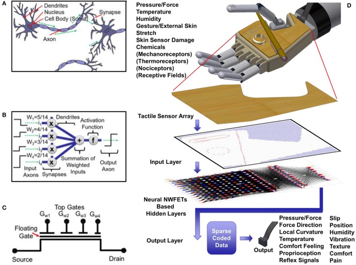
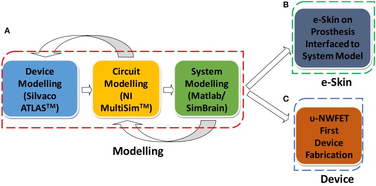
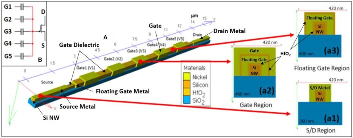
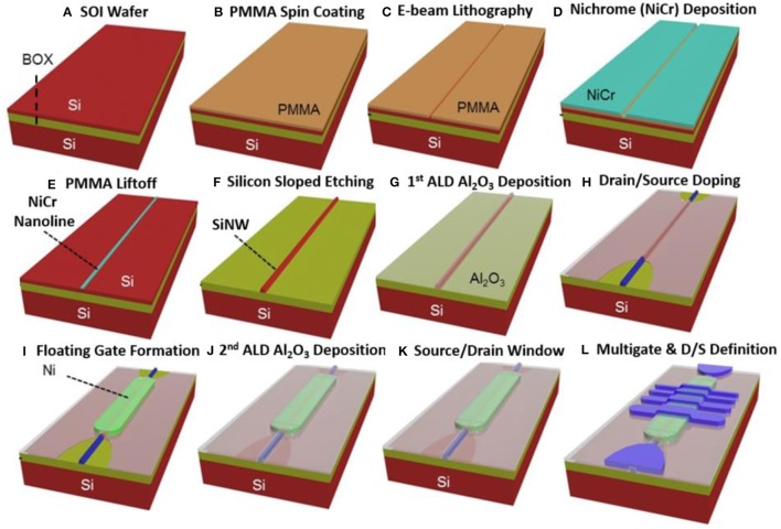
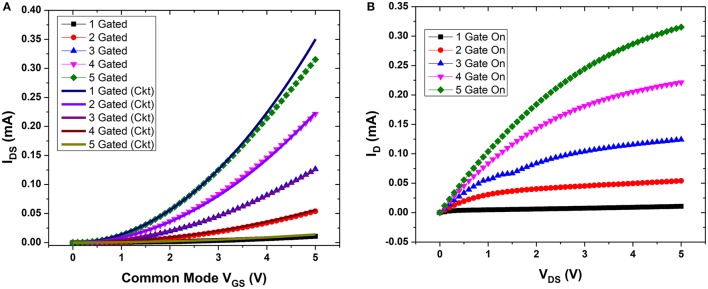
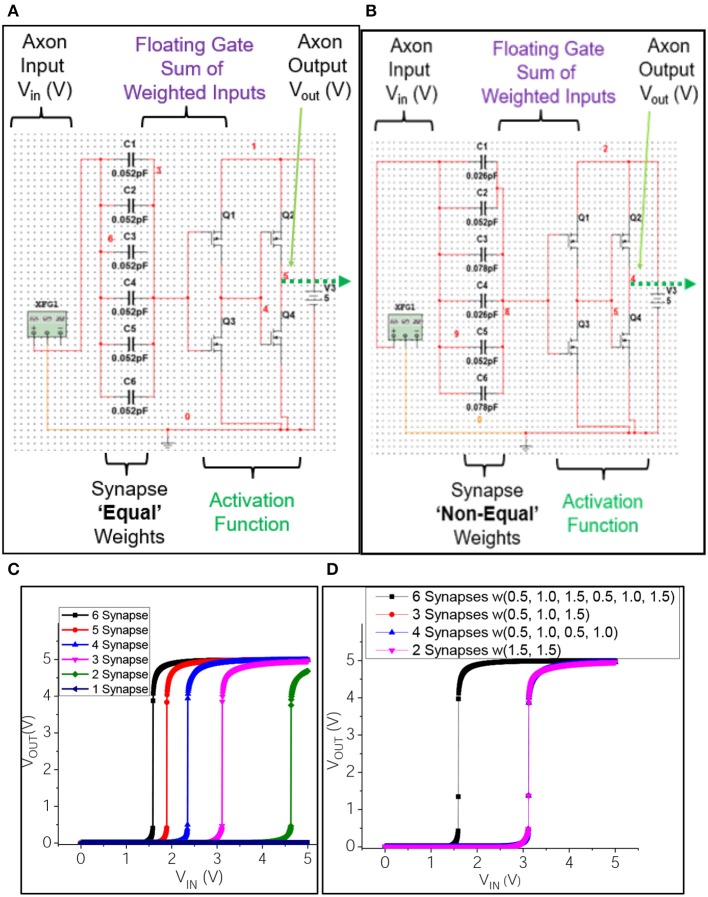
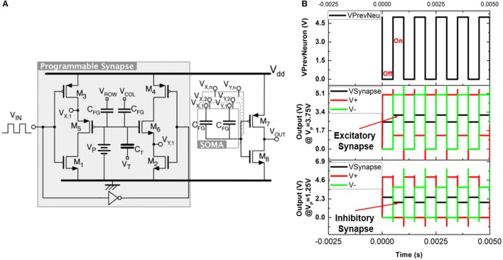
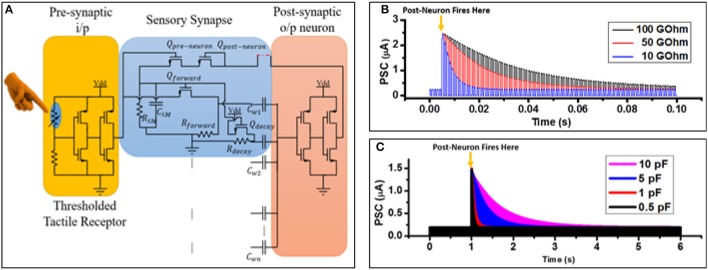
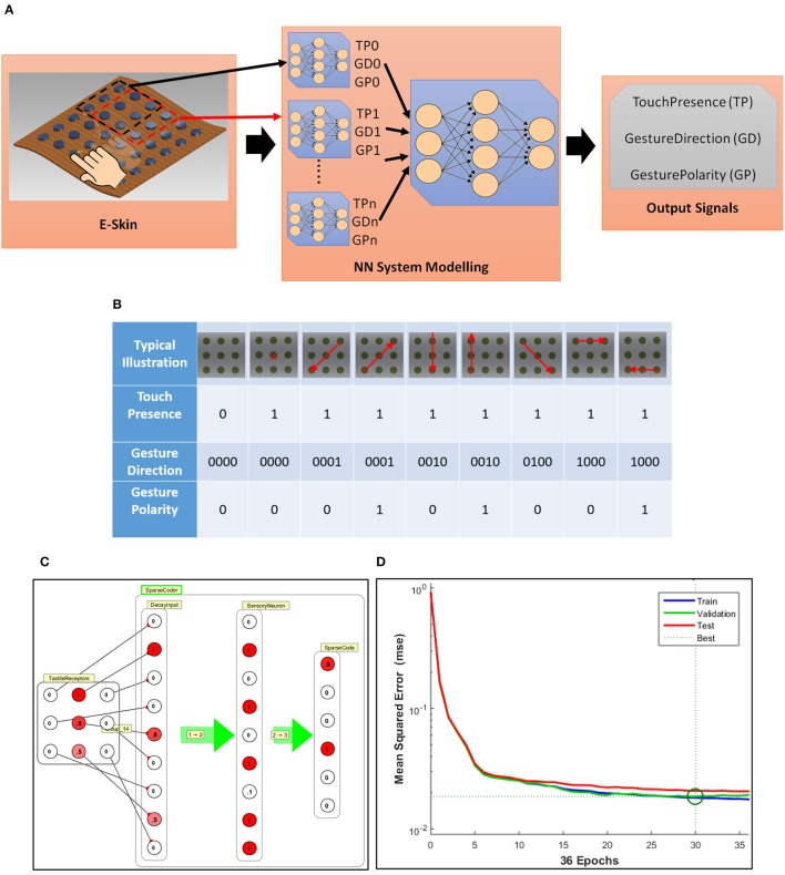
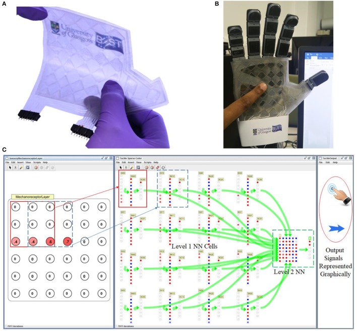
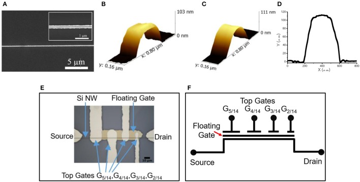
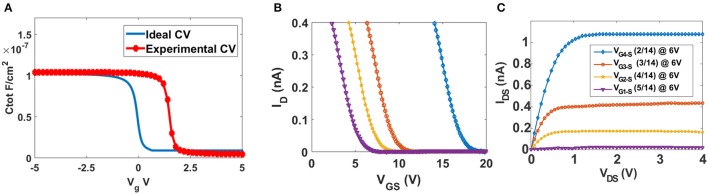
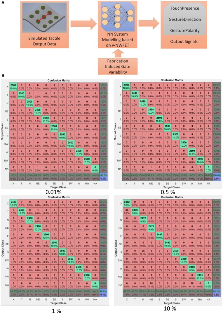
This paper presents novel Neural Nanowire Field Effect Transistors (υNWFETs) based hardware-implementable neural network (HNN) approach for tactile data processing in electronic skin (e-skin). The viability of Si nanowires (NWs) as the active material for υNWFETs in HNN is explored through modelling and demonstrated by fabricating the first device. Using υNWFETs to realize HNNs is an interesting approach as by printing NWs on large area flexible substrates it will be possible to develop a bendable tactile skin with distributed neural elements (for local data processing, as in biological skin) in the backplane. The modeling and simulation of υNWFET based devices show that the overlapping areas between individual gates and the floating gate determines the initial synaptic weights of the neural network - thus validating the working of υNWFETs as the building block for HNN. The simulation has been further extended to υNWFET based circuits and neuronal computation system and this has been validated by interfacing it with a transparent tactile skin prototype (comprising of 6x6 ITO based capacitive tactile sensors array) integrated on the palm of a 3D printed robotic hand. In this regard, a tactile data coding system is presented to detect touch gesture and the direction of touch. Following these simulation studies, a four-gated υNWFET is fabricated with Pt/Ti metal stack for gates, source and drain, Ni floating gate, and Al2O3 high-k dielectric layer. The currentvoltage characteristics of fabricated υNWFET devices confirm the dependence of turnoff voltages on the (synaptic) weight of each gate. The presented υNWFET approach is promising for a neuro-robotic tactile sensory system with distributed computing as well as numerous futuristic applications such as prosthetics, and electroceuticals.
Overview
The claims and statistics of this paper haven’t been checked yet.
Run the check — free, no account needed. It reads the open-access text and checks the sources it cites.
Integrity signals
Registry
Cites
Statistics
Figures
Verification
Claims the paper makes
The claims and statistics of this paper haven’t been checked yet.
Run the check — free, no account needed. It reads the open-access text and checks the sources it cites.
Claims other papers make about this one
Each is checked against this paper’s own text: does it say what the citing paper says it does?
The source backs part of the claim, not all of it — or backs it for a different population, condition or comparison.
In the citing paper
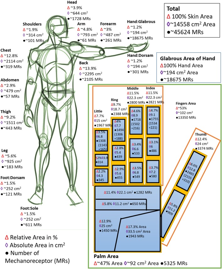
“Estimates of tactile fiber innervation in the current literature are few, often incomplete and inconsistent, and range from a total innervation of around 45,000 fibers (Taube Navaraj et al. 2017) into the millions (Grunwald 2017).”
From Tactile innervation densities across the whole body (2020) · cites this paper as Taube Navaraj et al. 2017
Experimental — accuracy not yet measured
Self-check
Percentages, sums and reported differences re-computed from the paper’s own numbers.
The self-check needs the paper’s full text.
Citations
Cites
A logical calculus of the ideas immanent in nervous activity
McCulloch, W. S., & Pitts, W. (1943) · The Bulletin of Mathematical Biophysics · doi:10.1007/bf02478259 · Cited by 18,566
Physics of Semiconductor Devices
Sze, S. M., & Ng, K. K. (2006) · doi:10.1002/0470068329 · Cited by 14,627
Human Memory: A Proposed System and its Control Processes
Atkinson, R. C., & Shiffrin, R. M. (1968) · Psychology of Learning and Motivation · doi:10.1016/s0079-7421(08)60422-3 · Cited by 7,216
Nanoscale Memristor Device as Synapse in Neuromorphic Systems
Jo, S. H., Chang, T., Ebong, I., Bhadviya, B. B., Mazumder, P., & Lu, W. (2010) · Nano Letters · doi:10.1021/nl904092h · Cited by 4,174 · cited 2×
“…thus far are based on devices such as memistor (Widrow and Hoff, 1960), spin-logic (Sengupta et al., 2015; Grollier et al., 2016), memristor (Jo et al., 2010), neuron MOSFET (Ishii et al., 1992; Kotani et al., 1998), analog circuit based neurons (Mead and Ismail, 2012), field programmable…”
BackgroundWIDROW, B., & HOFF, M. E. (1960) · doi:10.21236/ad0241531 · Cited by 4,009
Memristive devices for computing
Yang, J. J., Strukov, D. B., & Stewart, D. R. (2013) · Nature Nanotechnology · doi:10.1038/nnano.2012.240 · Cited by 3,885
Hammock, M. L., Chortos, A., Tee, B. C. ‐., Tok, J. B. ‐., & Bao, Z. (2013) · Advanced Materials · doi:10.1002/adma.201302240 · Cited by 2,396 · cited 3×
“) and their integration on large-area and flexible/conformable substrates (Dahiya and Valle, 2013; Dahiya et al., 2013a, 2015; Hammock et al., 2013; Lee et al., 2015; Yogeswaran et al., 2015; Polishchuk et al., 2016; Núñez et al., 2017).”
BackgroundCoding and use of tactile signals from the fingertips in object manipulation tasks
Johansson, R. S., & Flanagan, J. R. (2009) · Nature Reviews Neuroscience · doi:10.1038/nrn2621 · Cited by 2,063
Tactile Sensing—From Humans to Humanoids
Dahiya, R., Giorgio Metta, B., Valle, M., & Sandini, G. (2009) · IEEE Transactions on Robotics · doi:10.1109/tro.2009.2033627 · Cited by 1,890
Self-citationTee, B. C. K., Wang, C., Allen, R., & Bao, Z. (2012) · Nature Nanotechnology · doi:10.1038/nnano.2012.192 · Cited by 1,427
Johansson, R. S., & Vallbo, A. B. (1979) · The Journal of Physiology · doi:10.1113/jphysiol.1979.sp012619 · Cited by 1,291
User-interactive electronic skin for instantaneous pressure visualization
Wang, C., Hwang, D., Yu, Z., Takei, K., Park, J., Chen, T., Ma, B., & Javey, A. (2013) · Nature Materials · doi:10.1038/nmat3711 · Cited by 1,182
Restoring natural sensory feedback in real-time bidirectional hand prostheses
Raspopovic, S., Capogrosso, M., Petrini, F. M., Bonizzato, M., Rigosa, J., Di Pino, G., Carpaneto, J., Controzzi, M., Boretius, T., Fernandez, E., et al. (2014) · Science Translational Medicine · doi:10.1126/scitranslmed.3006820 · Cited by 1,001
Highly ordered nanowire arrays on plastic substrates for ultrasensitive flexible chemical sensors
McAlpine, M. C., Ahmad, H., Wang, D., & Heath, J. R. (2007) · Nature Materials · doi:10.1038/nmat1891 · Cited by 959
Patolsky, F., Timko, B. P., Yu, G., Fang, Y., Greytak, A. B., Zheng, G., & Lieber, C. M. (2006) · Science · doi:10.1126/science.1128640 · Cited by 832
Considerations for Ultimate CMOS Scaling
Kuhn, K. J. (2012) · IEEE Transactions on Electron Devices · doi:10.1109/ted.2012.2193129 · Cited by 680
Artificial neural networks in hardware: A survey of two decades of progress
Misra, J., & Saha, I. (2010) · Neurocomputing · doi:10.1016/j.neucom.2010.03.021 · Cited by 661
First spikes in ensembles of human tactile afferents code complex spatial fingertip events
Johansson, R. S., & Birznieks, I. (2004) · Nature Neuroscience · doi:10.1038/nn1177 · Cited by 651
A functional MOS transistor featuring gate-level weighted sum and threshold operations
Shibata, T., & Ohmi, T. (1992) · IEEE Transactions on Electron Devices · doi:10.1109/16.137325 · Cited by 612
Layer-by-Layer Assembly of Nanowires for Three-Dimensional, Multifunctional Electronics
Javey, A., Nam, S., Friedman, R. S., Yan, H., & Lieber, C. M. (2007) · Nano Letters · doi:10.1021/nl063056l · Cited by 597
Information Coding in the Vertebrate Olfactory System
Buck, L. B. (1996) · Annual Review of Neuroscience · doi:10.1146/annurev.ne.19.030196.002505 · Cited by 539
Programmable nanowire circuits for nanoprocessors
Yan, H., Choe, H. S., Nam, S., Hu, Y., Das, S., Klemic, J. F., Ellenbogen, J. C., & Lieber, C. M. (2011) · Nature · doi:10.1038/nature09749 · Cited by 524
Fuster, J. M. (1997) · Trends in Neurosciences · doi:10.1016/s0166-2236(97)01128-4 · Cited by 516
Dahiya, R., & Valle, M. (2012) · Springer eBooks · doi:10.1007/978-94-007-0579-1 · Cited by 459
Self-citationMultiple models to capture the variability in biological neurons and networks
Marder, E., & Taylor, A. L. (2011) · Nature Neuroscience · doi:10.1038/nn.2735 · Cited by 451
Spintronic Nanodevices for Bioinspired Computing
Grollier, J., Querlioz, D., & Stiles, M. D. (2016) · Proceedings of the IEEE · doi:10.1109/jproc.2016.2597152 · Cited by 447
Directions Toward Effective Utilization of Tactile Skin: A Review
Dahiya, R., Mittendorfer, P., Valle, M., Cheng, G., & Lumelsky, V. (2013) · IEEE Sensors Journal · doi:10.1109/jsen.2013.2279056 · Cited by 435
Self-citationArray-based architecture for FET-based, nanoscale electronics
DeHon, A. M. (2003) · IEEE Transactions on Nanotechnology · doi:10.1109/tnano.2003.808508 · Cited by 370
Barlow, H. B. (1981) · Proceedings of the Royal Society B Biological Sciences · doi:10.1098/rspb.1981.0022 · Cited by 367
Whole‐body mapping of spatial acuity for pain and touch
Mancini, F., Bauleo, A., Cole, J., Lui, F., Porro, C. A., Haggard, P., & Iannetti, G. D. (2014) · Annals of Neurology · doi:10.1002/ana.24179 · Cited by 330
Energy‐Autonomous, Flexible, and Transparent Tactile Skin
García‐Núñez, C., Navaraj, W. T., Polat, E. O., & Dahiya, R. (2017) · Advanced Functional Materials · doi:10.1002/adfm.201606287 · Cited by 316
Self-citationAnanthanarayanan, R., Esser, S. K., Simon, H. D., & Modha, D. S. (2009) · International Conference for High Performance Computing, Networking, Storage and Analysis (SC) · doi:10.1145/1654059.1654124 · Cited by 262
Bauer, S. (2013) · Nature Materials · doi:10.1038/nmat3759 · Cited by 235
1957 IRE WESCON Convention Record
(1957) · Proceedings of the IRE · doi:10.1109/jrproc.1957.278542 · Cited by 232
Nanowire transistor arrays for mapping neural circuits in acute brain slices
Qing, Q., Pal, S. K., Tian, B., Duan, X., Timko, B. P., Cohen‐Karni, T., Murthy, V. N., & Lieber, C. M. (2010) · Proceedings of the National Academy of Sciences · doi:10.1073/pnas.0914737107 · Cited by 204
New materials and advances in making electronic skin for interactive robots
Yogeswaran, N., Dang, W., Navaraj, W. T., Shakthivel, D., Khan, S., Polat, E. O., Gupta, S., Heidari, H., Kaboli, M., Lorenzelli, L., et al. (2015) · Advanced Robotics · doi:10.1080/01691864.2015.1095653 · Cited by 187
Self-citationNanoionics-Based Three-Terminal Synaptic Device Using Zinc Oxide
Pillai, P. B., & Souza, M. M. D. (2016) · ACS Applied Materials & Interfaces · doi:10.1021/acsami.6b13746 · Cited by 169
Within touch of artificial skin
Boland, J. J. (2010) · Nature Materials · doi:10.1038/nmat2861 · Cited by 164
McAlpine, M. C., Friedman, R. S., & Lieber, C. M. (2005) · Proceedings of the IEEE · doi:10.1109/jproc.2005.850308 · Cited by 128
Boahen, K. A. (2017) · Computing in Science & Engineering · doi:10.1109/mcse.2017.33 · Cited by 105
Tactile-Data Classification of Contact Materials Using Computational Intelligence
Decherchi, S., Gastaldo, P., Dahiya, R., Valle, M., & Zunino, R. (2011) · IEEE Transactions on Robotics · doi:10.1109/tro.2011.2130030 · Cited by 100
Self-citationSpin orbit torque based electronic neuron
Sengupta, A., Choday, S. H., Kim, Y., & Roy, K. (2015) · Applied Physics Letters · doi:10.1063/1.4917011 · Cited by 88
“Analog VLSI Implementation of Neural Systems”
(1990) · Integration · doi:10.1016/0167-9260(90)90024-u · Cited by 88
Developing Electronic Skin with the Sense of Touch
Dahiya, R., Navaraj, W. T., Khan, S., & Polat, E. O. (2015) · Information Display · doi:10.1002/j.2637-496x.2015.tb00824.x · Cited by 64
Self-citationPOSFET tactile sensing arrays using CMOS technology
Dahiya, R., Adami, A., Collini, C., & Lorenzelli, L. (2013) · Sensors and Actuators A Physical · doi:10.1016/j.sna.2013.02.007 · Cited by 64
Self-citationKaboli, M., Armando De La Rosa, T., Walker, R., & Cheng, G. (2015) · IEEE-RAS International Conference on Humanoid Robots (Humanoids) · doi:10.1109/humanoids.2015.7363508 · Cited by 63
Nanowire electrodes for high-density stimulation and measurement of neural circuits
Robinson, J. T., Jorgolli, M., & Park, H. (2013) · Frontiers in Neural Circuits · doi:10.3389/fncir.2013.00038 · Cited by 62
Development of ultra-high density silicon nanowire arrays for electronics applications
Wang, D., Sheriff, B. A., McAlpine, M. C., & Heath, J. R. (2008) · Nano Research · doi:10.1007/s12274-008-8005-8 · Cited by 57
Proportion of Skin Surface Area of Children and Young Adults from 2 to 18 Years Old
Boniol, M., Verriest, J.-P., Pedeux, R., & Doré, J. (2007) · Journal of Investigative Dermatology · doi:10.1038/sj.jid.5701032 · Cited by 46
Clock-controlled neuron-MOS logic gates
Kotani, K., Shibata, T., Imai, M., & Ohmi, T. (1998) · IEEE Transactions on Circuits and Systems II Analog and Digital Signal Processing · doi:10.1109/82.663810 · Cited by 42
Lee, W. W., Kukreja, S. L., & Thakor, N. V. (2015) · IEEE Biomedical Circuits and Systems Conference (BioCAS) · doi:10.1109/biocas.2015.7348412 · Cited by 42
2015 IEEE Biomedical Circuits and Systems Conference (BioCAS)
(2015) · doi:10.1109/biocas34748.2015 · Cited by 40
Bioengineered nerve conduits and wraps for peripheral nerve repair of the upper limb
Thomson, S., Ng, N. Y., Riehle, M. O., Kingham, P. J., Dahlin, L. B., Wiberg, M., & Hart, A. M. (2022) · Cochrane Database of Systematic Reviews · doi:10.1002/14651858.cd012574.pub2 · Cited by 39
Basavanna, M. (2015) · Jaypee Brothers Medical Publishers (P) Ltd. eBooks · doi:10.5005/jp/books/12408_5 · Cited by 37
Sparsity and Compressed Coding in Sensory Systems
Barranca, V. J., Kovačič, G., Zhou, D., & Cai, D. (2014) · PLoS Computational Biology · doi:10.1371/journal.pcbi.1003793 · Cited by 28
Multisensory Smart Glove for Tactile Feedback in Prosthetic Hand
Полищук, А. А., Navaraj, W. T., Heidari, H., & Dahiya, R. (2016) · Procedia Engineering · doi:10.1016/j.proeng.2016.11.471 · Cited by 28
Self-citationHardware-backpropagation learning of neuron MOS neural networks
Ishii, I., Shibata, Kosaka, & Ohmi (1992) · Technical digest - International Electron Devices Meeting/Technical digest · doi:10.1109/iedm.1992.307395 · Cited by 27
A SPICE-Compatible New Silicon Nanowire Field-Effect Transistors (SNWFETs) Model
Lee, S. H., Yu, Y. S., Hwang, S. W., & Ahn, D. (2009) · IEEE Transactions on Nanotechnology · doi:10.1109/tnano.2009.2019724 · Cited by 22
Learning with discrete multivalued neurons
Zoran Obradovic, A., & Parberry, I. (1994) · Journal of Computer and System Sciences · doi:10.1016/s0022-0000(05)80055-8 · Cited by 22
Simbrain 3.0: A flexible, visually-oriented neural network simulator
Tosi, Z., & Yoshimi, J. (2016) · Neural Networks · doi:10.1016/j.neunet.2016.07.005 · Cited by 21
Computing with discrete multi-valued neurons
Zoran Obradovic, A., & Parberry, I. (1992) · Journal of Computer and System Sciences · doi:10.1016/0022-0000(92)90035-h · Cited by 18
Compensation of Sensors Nonlinearity with Neural Networks
Cotton, N. J., & Wilamowski, B. M. (2010) · IEEE International Conference on Advanced Information Networking and Applications (AINA) · doi:10.1109/aina.2010.170 · Cited by 16
Can HPE’s "The Machine" deliver?
Courtland, R. E. (2015) · IEEE Spectrum · doi:10.1109/mspec.2016.7367460 · Cited by 8
ROLE OF INTERFACE CHARGES ON HIGH-K BASED POLY-SI AND METAL GATE NANO-SCALE MOSFETS
Shashank, N., & Singh, V. (2011) · DOAJ (DOAJ: Directory of Open Access Journals) · Cited by 8
Bioengineered nerve conduits and wraps for peripheral nerve repair of the upper limb
Thomson, S., Ng, N. Y., Riehle, M. O., Kingham, P. J., Dahlin, L. B., Wiberg, M., & Hart, A. M. (2017) · Cochrane Database of Systematic Reviews · doi:10.1002/14651858.cd012574 · Cited by 7
VLS growth mechanism of Si-nanowires for flexible electronics
Shakthivel, D., Navaraj, W. T., Raghavan, S., & Dahiya, R. (2015) · Conference on Ph.D. Research in Microelectronics and Electronics · doi:10.1109/prime.2015.7251407 · Cited by 6
Self-citationModelling of nanowire FETs based neural network for tactile pattern recognition in E-skin
Navaraj, W. T., Liu, F., Vilouras, A., Shaktivel, D., García‐Núñez, C., Heidari, H., Labeau, F., Gregory, D. H., & Dahiya, R. (2016) · IEEE Biomedical Circuits and Systems Conference (BioCAS) · doi:10.1109/biocas.2016.7833859 · Cited by 3
Self-citationTransfer Printing Si Nanowires for Flexible Large Area Electronics
Shakthivel, D., Navaraj, W. T., García‐Núñez, C., Liu, F., & Dahiya, R. (2016) · Cited by 3
Self-citationMetal-assisted chemical etched Si nanowires for high-performance large area flexible electronics
Navaraj, W. T., Shakthivel, D., García‐Núñez, C., Liu, F., Gregory, D. H., & Dahiya, R. (2017) · ENLIGHTEN (Jurnal Bimbingan dan Konseling Islam) · Cited by 1
Self-citation
Cited by
Sorted by citations
Wang, M., Luo, Y., Wang, T., Wan, C., Pan, L., Pan, S., He, K., Neo, A., & Chen, X. (2021) · Advanced Materials · doi:10.1002/adma.202003014 · Cited by 451
Tactile innervation densities across the whole body
Corniani, G., & Saal, H. P. (2020) · Journal of Neurophysiology · doi:10.1152/jn.00313.2020 · Cited by 396
Ultra-thin chips for high-performance flexible electronics
Gupta, S., Navaraj, W. T., Lorenzelli, L., & Dahiya, R. (2018) · npj Flexible Electronics · doi:10.1038/s41528-018-0021-5 · Cited by 373
Self-citationEnergy autonomous electronic skin
García Núñez, C., Manjakkal, L., & Dahiya, R. (2019) · npj Flexible Electronics · doi:10.1038/s41528-018-0045-x · Cited by 332
“i Image of the prosthetic/robotic hand with e-skin.(8) C.”
BackgroundSelf-citationBiodegradable Materials for Sustainable Health Monitoring Devices
Hosseini, E. S., Dervin, S., Ganguly, P., & Dahiya, R. (2020) · ACS Applied Bio Materials · doi:10.1021/acsabm.0c01139 · Cited by 341
Self-citation
Metadata
- Authors
- Taube Navaraj, W., García Núñez, C., Shakthivel, D., Vinciguerra, V., Labeau, F., Gregory, D. H., & Dahiya, R.
- Affiliations
- University of Glasgow (GB)
- STMicroelectronics (Italy) (IT)
- McGill University (CA)
- Corresponding author
- Dahiya, Ravinder
- Venue
- Frontiers in Neuroscience
- Publisher
- Frontiers Media SA
- Published
- 2017-09-20
- Volume
- 11
- Pages
- 501-501
- ISSN
- 1662-453X (ISSN-L)
- PMC
- PMC5611376
- OpenAlex
- W2755222108
- Cited by
- 127
- References
- 70
- Citations by year
- 2026: 4 · 2025: 9 · 2024: 10 · 2023: 7 · 2022: 16 · 2021: 21 · 2020: 28 · 2019: 15 · 2018: 13 · 2017: 4
- FWCI
- 6.82
- Type
- journal article
- Language
- en
- Open access
- gold
- doi.org
- Licence
- cc-by
- Locations
- Frontiers in Neuroscience (publishedVersion, cc-by)
- Europe PMC (PubMed Central) (publishedVersion, cc-by)
- PubMed Central (publishedVersion, cc-by)
- PubMed (publishedVersion)
- Nottingham Trent University's Institutional Repository (Nottingham Trent Repository) (acceptedVersion)
- ENLIGHTEN (Jurnal Bimbingan dan Konseling Islam) (acceptedVersion)
- DOAJ (DOAJ: Directory of Open Access Journals) (submittedVersion)
- eScholarship@McGill (McGill) (submittedVersion, cc-by)
- Funders
- Engineering and Physical Sciences Research Council (EP/M002527/1)
- Topics
- Physical Sciences › Engineering › Electrical and Electronic Engineering › Advanced Memory and Neural Computing
- Physical Sciences › Materials Science › Electronic, Optical and Magnetic Materials › Nanowire Synthesis and Applications
- Physical Sciences › Engineering › Electrical and Electronic Engineering › Advancements in Semiconductor Devices and Circuit Design
- Keywords
- nanowire field-effect transistors, silicon nanowires, electronic skin, tactile sensing, robotic hand, synaptic weights, floating gate, capacitive tactile sensor, neurorobotics, flexible electronics, high-k dielectrics
About these checks
Registry, retraction, Cites and statistics results are computed, not judged, with one exception: a printed reference that no index lists is read once by a model before it counts as a citation error. Claims are extracted by a model and kept only when their quote appears verbatim in the text; each cited source is then checked, with a model’s help, for whether it says what the claim relies on. Those verdicts can be wrong — read the claim’s quote and the cited source before relying on one.
Statistics and arithmetic are recomputed, not judged.
Confidence bands are shown only for fields calibrated on our annotated test set. None is calibrated yet, so no band is shown.
What counts as a claim ›How we measure confidence ›How we check this ›
Are you an author, or do you see a problem with this page? Request a review
