

The DOI matches its Crossref record; 60 of the 60 references it cites were found in a registry or an index.
Hybrid Integrated Platforms for Silicon Photonics
Open accessAbstract
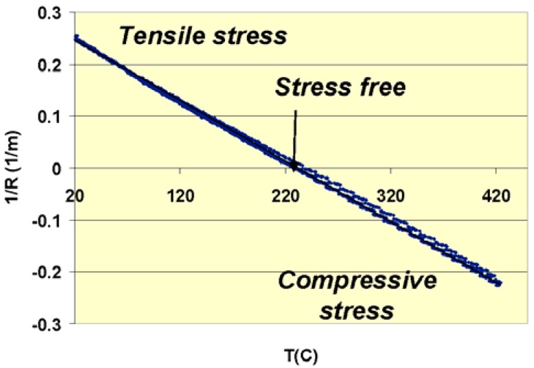
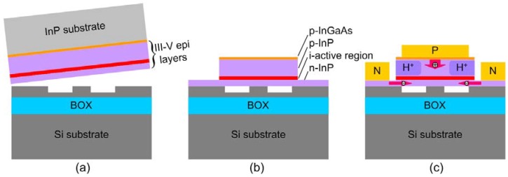
A review of recent progress in hybrid integrated platforms for silicon photonics is presented. Integration of III-V semiconductors onto silicon-on-insulator substrates based on two different bonding techniques is compared, one comprising only inorganic materials, the other technique using an organic bonding agent. Issues such as bonding process and mechanism, bonding strength, uniformity, wafer surface requirement, and stress distribution are studied in detail. The application in silicon photonics to realize high-performance active and passive photonic devices on low-cost silicon wafers is discussed. Hybrid integration is believed to be a promising technology in a variety of applications of silicon photonics.
Overview
The claims and statistics of this paper haven’t been checked yet.
Run the check — free, no account needed. It reads the open-access text and checks the sources it cites.
Integrity signals
Registry
Cites
Statistics
Figures
Verification
Claims the paper makes
The claims and statistics of this paper haven’t been checked yet.
Run the check — free, no account needed. It reads the open-access text and checks the sources it cites.
Claims other papers make about this one
Each is checked against this paper’s own text: does it say what the citing paper says it does?
The cited source says what the claim attributes to it.
In the citing paper
“Integration proximity of the (dissimilar) materials in direct bonding facilitates superior optical coupling and heat transportation between them56.”
From Roadmapping the next generation of silicon photonics (2024) · cites this paper as [56]
Self-check
Percentages, sums and reported differences re-computed from the paper’s own numbers.
The self-check needs the paper’s full text.
Citations
Cites
Device Requirements for Optical Interconnects to Silicon Chips
Miller, D. A. B. (2009) · Proceedings of the IEEE · doi:10.1109/jproc.2009.2014298 · Cited by 2,000
Electrically pumped hybrid AlGaInAs-silicon evanescent laser
Fang, A. W., Park, H., Cohen, O., Jones, R., Paniccia, M. J., & Bowers, J. E. (2006) · Optics Express · doi:10.1364/oe.14.009203 · Cited by 1,244
Self-citationBonding of silicon wafers for silicon-on-insulator
Maszara, W., Goetz, G., Caviglia, A. L., & McKitterick, J. B. (1988) · Journal of Applied Physics · doi:10.1063/1.342443 · Cited by 878
Gösele, U., & Tong, Q.-Y. (1998) · Annual Review of Materials Science · doi:10.1146/annurev.matsci.28.1.215 · Cited by 600
SemiConductor Wafer Bonding: Science and Technology
Tong, Q., & Gösele, U. (1998) · Cited by 555
Campenhout, J. V., Romeo, P. R., Régreny, P., Seassal, C., Thourhout, D. V., Verstuyft, S., Cioccio, L. D., Fédéli, J.-M., Lagahe, C., & Baets, R. (2007) · Optics Express · doi:10.1364/oe.15.006744 · Cited by 513
Self-citationNiklaus, F., Stemme, G., Lu, J., & Gutmann, R. J. (2006) · Journal of Applied Physics · doi:10.1063/1.2168512 · Cited by 473
Magneto-optical isolator with silicon waveguides fabricated by direct bonding
Shoji, Y., Mizumoto, T., Yokoi, H., Hsieh, I.-W., & Osgood, R. M. (2008) · Applied Physics Letters · doi:10.1063/1.2884855 · Cited by 336
Miller, D. A. B., & Özaktaş, H. M. (1997) · Journal of Parallel and Distributed Computing · doi:10.1006/jpdc.1996.1285 · Cited by 290
Plasma-assisted InP-to-Si low temperature wafer bonding
Pasquariello, D. M., & Hjort, K. (2002) · IEEE Journal of Selected Topics in Quantum Electronics · doi:10.1109/2944.991407 · Cited by 250
Cited by
Sorted by citations
Items 101–200 of 316
Hybrid Materials for Integrated Photonics
Bettotti, P. (2014) · Advances in Optics · doi:10.1155/2014/891395 · Cited by 27
Yang, Y., Djogo, G., Haque, M., Herman, P. R., & Poon, J. K. S. (2017) · Optics Express · doi:10.1364/oe.25.005758 · Cited by 27
Hybrid material integration for active photonic applications
Chen, C., Chen, Y., Fang, Z., Ge, R., Wu, J., & Chen, X. (2024) · APL Photonics · doi:10.1063/5.0187924 · Cited by 25
Low-Temperature Bonding for Silicon-Based Micro-Optical Systems
Qin, Y., Howlader, M. M. R., & Deen, M. J. (2015) · Photonics · doi:10.3390/photonics2041164 · Cited by 25
Inter-layer light transition in hybrid III-V/Si waveguides integrated by µ-transfer printing
Kou, R., Hiratani, T., Yagi, H., Kuwatsuka, H., Yen, T.-H., Okano, M., Ohno, M., Kawashima, H., Suzuki, K., Fujiwara, N., et al. (2020) · Optics Express · doi:10.1364/oe.394492 · Cited by 25
On the Optoelectronic Mechanisms Ruling Ti‐hyperdoped Si Photodiodes
García-Hemme, E., Caudevilla, D., Algaidy, S., Pérez-Zenteno, F., García-Hernansanz, R., Olea, J., Pastor, D., del Prado, '., Andrés, E. S., Martil, I., et al. (2021) · Advanced Electronic Materials · doi:10.1002/aelm.202100788 · Cited by 25
Energy-Efficient Hybrid Silicon Electroabsorption Modulator for 40-Gb/s 1-V Uncooled Operation
Tang, Y., Peters, J., & Bowers, J. E. (2012) · IEEE Photonics Technology Letters · doi:10.1109/lpt.2012.2212702 · Cited by 25
Self-citationFujii, T., Hiraki, T., Aihara, T., Nishi, H., Takeda, K., Sato, T., Kakitsuka, T., Tsuchizawa, T., & Matsuo, S. (2021) · Applied Sciences · doi:10.3390/app11041801 · Cited by 24
III-V/Si wafer bonding using transparent, conductive oxide interlayers
Tamboli, A. C., van Hest, M. F. A. M., Steiner, M. A., Essig, S., Perl, E. E., Norman, A. G., Bosco, N., & Stradins, P. (2015) · Applied Physics Letters · doi:10.1063/1.4923444 · Cited by 24
Beyond the detection limit: A review of high-Q optical ring resonator sensors
Butt, M. A. (2025) · Materials Today Physics · doi:10.1016/j.mtphys.2025.101873 · Cited by 23
Materials for ultra-efficient, high-speed optoelectronics
Moody, G., & Islam, M. S. (2022) · MRS Bulletin · doi:10.1557/s43577-022-00337-y · Cited by 23
Butt, M. A., & Mateos, X. (2024) · Applied Sciences · doi:10.3390/app14146365 · Cited by 22
Ahn, G. H., White, A. D., Kim, H., Higashitarumizu, N., Mayor, F. M., Herrmann, J. F., Jiang, W., Multani, K. K. S., Safavi-Naeini, A. H., Javey, A., et al. (2023) · Optica · doi:10.1364/optica.475387 · Cited by 22
Sirbu, B., Eichhammer, Y., Oppermann, H. H., Tekin, T., Kraft, J., Sidorov, V., Yin, X. L., Bauwelinck, J., Neumeyr, C., & Soares, F. M. (2019) · IEEE Electronic Components and Technology Conference (ECTC) · doi:10.1109/ectc.2019.00165 · Cited by 21
Integrated Hybrid Silicon Transmitters
Jain, S. R., Tang, Y., Chen, H., Sysak, M. N., & Bowers, J. E. (2011) · Journal of Lightwave Technology · doi:10.1109/jlt.2011.2174028 · Cited by 21
Self-citationPhotonics-Assisted Beamforming for 5G Communications
Serafino, G., Porzi, C., Falconi, F., Pinna, S., Puleri, M., D’Errico, A., Bogoni, A., & Ghelfi, P. (2018) · IEEE Photonics Technology Letters · doi:10.1109/lpt.2018.2874468 · Cited by 20
A Review of the Reliability of Integrated IR Laser Diodes for Silicon Photonics
Buffolo, M., Santi, C. D., Norman, J., Shang, C., Bowers, J. E., Meneghesso, G., Zanoni, E., & Meneghini, M. (2021) · Electronics · doi:10.3390/electronics10222734 · Cited by 20
Self-citationModulators in Silicon Photonics—Heterogenous Integration & and Beyond
Mulcahy, J., Peters, F. H., & Dai, X. (2022) · Photonics · doi:10.3390/photonics9010040 · Cited by 21
Novel hybrid plasmonic-based directional coupler on InP substrate
Nikoufard, M., Heydari, N., Pourgholi, S., & Rostami-Khomami, A. (2016) · Photonics and Nanostructures - Fundamentals and Applications · doi:10.1016/j.photonics.2016.08.002 · Cited by 20
Micro-transfer printing of O-band InAs/GaAs quantum-dot SOAs on silicon photonic integrated circuits
Liu, Y., Zhang, J., Bogaert, L., Soltanian, E., Delli, E., Morozov, K., Mikhrin, S. S., Rimböck, J., Lepage, G., Verheyen, P., et al. (2025) · Photonics Research · doi:10.1364/prj.545946 · Cited by 19
Self-citationUnbiased Plasmonic-Assisted Integrated Graphene Photodetectors
Vangelidis, I., Bellas, D. V., Suckow, S., Dabos, G., Castilla, S., Koppens, F. H. L., Ferrari, A. C., Pleros, N., & Lidorikis, E. (2022) · ACS Photonics · doi:10.1021/acsphotonics.2c00100 · Cited by 19
Integration of GaAs waveguides on a silicon substrate for quantum photonic circuits
Shadmani, A., Thomas, R. A., Liu, Z., Papon, C., Heck, M. J. R., Volet, N., Scholz, S., Wieck, A. D., Ludwig, A., Lodahl, P., et al. (2022) · Optics Express · doi:10.1364/oe.467920 · Cited by 19
Research Toward a Heterogeneously Integrated InGaN Laser on Silicon
Kamei, T., Kamikawa, T., Araki, M., DenBaars, S. P., Nakamura, S., & Bowers, J. E. (2019) · physica status solidi (a) · doi:10.1002/pssa.201900770 · Cited by 19
Self-citationChen, Y., Zhu, S., Wei, Q., Xia, Y., Li, A., Yin, J., & Liu, Z. G. (2018) · Applied Physics Letters · doi:10.1063/1.5018226 · Cited by 19
Advancements in transfer printing techniques and their applications in photonic integrated circuits
Yu, C., Zhang, M., Liang, L., Li, Q., Chen, Y., Lei, Y., Wang, Y., Song, Y., Qiu, C., Jia, P., et al. (2025) · Light Science & Applications · doi:10.1038/s41377-025-02064-w · Cited by 18
Degradation Mechanisms of Heterogeneous III-V/Silicon 1.55- $\mu \text{m}$ DBR Laser Diodes
Buffolo, M., Meneghini, M., Santi, C. D., Davenport, M. L., Bowers, J. E., Meneghesso, G., & Zanoni, E. (2017) · IEEE Journal of Quantum Electronics · doi:10.1109/jqe.2017.2714582 · Cited by 18
Self-citationOn-Chip Photonic Crystal Surface-Emitting Membrane Lasers
Zhou, W., Liu, S., Ge, X., Zhao, D., Yang, H., Reuterskiöld-Hedlund, C., & Hammar, M. (2019) · IEEE Journal of Selected Topics in Quantum Electronics · doi:10.1109/jstqe.2019.2902904 · Cited by 17
Heterogeneously Integrated Photodiodes on Silicon
Beling, A., & Campbell, J. C. (2015) · IEEE Journal of Quantum Electronics · doi:10.1109/jqe.2015.2480595 · Cited by 16
Research progress of III–V laser bonding to Si
Ren, B., Hou, Y., & Liang, Y. (2016) · Journal of Semiconductors · doi:10.1088/1674-4926/37/12/124001 · Cited by 16
Gong, K., Sun, C., Xiong, B., Han, Y., Hao, Z., Wang, J., Wang, L., & Li, H. (2017) · AIP Advances · doi:10.1063/1.4975345 · Cited by 16
Self-assembled monolayer assisted bonding of Si and InP
Bakish, I., Artel, V., Ilovitsh, T., Shubely, M., Ben-Ezra, Y., Zadok, A., & Sukenik, C. N. (2012) · Optical Materials Express · doi:10.1364/ome.2.001141 · Cited by 15
Spectral Interferometry with Frequency Combs
Twayana, K., Rebolledo‐Salgado, I., Deriushkina, E., Schröder, J., & Karlsson, M. (2022) · Micromachines · doi:10.3390/mi13040614 · Cited by 14
Highly Accurate Docking of a Photonic Crystal Nanolaser to a SiNx Waveguide by Transfer Printing
Lu, T.-W., Lin, Y.-C., & Lee, P.-T. (2023) · ACS Photonics · doi:10.1021/acsphotonics.3c00411 · Cited by 14
Zhang, R., Zhao, B., Huang, K., You, T., Jia, Q., Lin, J., Zhang, S., Yan, Y., Yi, A., Zhou, M., et al. (2018) · AIP Advances · doi:10.1063/1.5030776 · Cited by 14
Ultrafast Carbon Nanotube Photodetectors with Bandwidth over 60 GHz
Wu, W., Yang, F., Fang, X., Cai, X., Liu, X., Zhang, F., & Wang, S. (2023) · ACS Photonics · doi:10.1021/acsphotonics.2c01626 · Cited by 14
1D Photonic Crystals: Principles and Applications in Silicon Photonics
Han, L. (2018) · InTech eBooks · doi:10.5772/intechopen.71753 · Cited by 14
A p-Si/n-GaN diode fabricated by nanomembrane lift-off and transfer-print technique
Liu, Y., Wang, L., Wang, L., Wu, X., Hao, Z., Yu, J., Luo, Y., Sun, C., Han, Y., Xiong, B., et al. (2019) · Semiconductor Science and Technology · doi:10.1088/1361-6641/ab408b · Cited by 14
18 Tb/s photonic digital signal processor for real time video image processingPreprint
Tan, M., Xu, X., Boes, A., Corcoran, B., Nguyen, T. G., Chu, S. T., Little, B. E., Morandotti, R., Wu, J., Mitchell, A., et al. (2022) · Research Square · doi:10.21203/rs.3.rs-1775424/v1 · Cited by 14
Room temperature wafer direct bonding of smooth Si surfaces recovered by Ne beam surface treatments
Kurashima, Y., Maeda, A., & Takagi, H. (2013) · Applied Physics Letters · doi:10.1063/1.4812742 · Cited by 13
Yaita, J., Tsuji, T., Hatano, M., & Iwasaki, T. (2018) · Applied Physics Express · doi:10.7567/apex.11.045501 · Cited by 13
Nonlinear Nanophotonics With 2D Transition Metal Dichalcogenides
Chen, H., Tang, Y., Jiang, T., & Li, G. (2018) · Elsevier eBooks · doi:10.1016/b978-0-12-803581-8.11340-2 · Cited by 13
Colossal Terahertz Emission with Ultrafast Tunability Based on Van der Waals Ferroelectric NbOI2
Subedi, S., Liu, W., Fang, W., Fox, C., Zhai, Z., Fei, F., Ping, Y., Lv, B., & Xiao, J. (2025) · Advanced Optical Materials · doi:10.1002/adom.202403471 · Cited by 12
Power and scalability analysis of multi-plane optical interconnection networks
Cerutti, I., Andriolli, N., Raponi, P. G., Scaffardi, M., Liboiron-Ladouceur, O., Bogoni, A., & Castoldi, P. (2012) · IET Optoelectronics · doi:10.1049/iet-opt.2010.0114 · Cited by 12
Two-Mode Converters at 1.3 μm Based on Multimode Interference Couplers on InP Substrates
Fei, G., Lu, D., Zhang, R., Wang, H., Wei, W., & Ji, C. (2016) · Chinese Physics Letters · doi:10.1088/0256-307x/33/2/024203 · Cited by 12
Moscoso‐Mártir, A., Müller, J., Islamova, E., Merget, F., & Witzens, J. (2017) · Scientific Reports · doi:10.1038/s41598-017-12023-0 · Cited by 12
Optical Kerr nonlinear effect in InP-based hybrid plasmonic waveguides
Firouzabadi, M. D., Nikoufard, M., & Tavakoli, M. B. (2017) · Optical and Quantum Electronics · doi:10.1007/s11082-017-1226-x · Cited by 12
Thin Films - Growth, Characterization and Electrochemical Applications
Sarf, F., Yakar, E., & Er, İ. K. (2023) · IntechOpen eBooks · doi:10.5772/intechopen.107556 · Cited by 11
Dhiman, A. (2013) · IOSR Journal of Applied Physics · doi:10.9790/4861-0356779 · Cited by 11
Ultra-Sharp and Highly Tolerant Waveguide Bends for InP Photonic Membrane Circuits
Jiao, Y., Liu, J., Mejia, A. M., Shen, L., & van der Tol, J. J. G. M. (2016) · IEEE Photonics Technology Letters · doi:10.1109/lpt.2016.2565607 · Cited by 11
Role of surface passivation in integrated sub-bandgap silicon photodetection
Gherabli, R., Grajower, M. Y., Shappir, J., Mazurski, N., Vofsi, M., Inbar, N., Khurgin, J. B., & Levy, U. (2020) · Optics Letters · doi:10.1364/ol.388983 · Cited by 11
Beling, A., Cross, A. S., Piels, M., Peters, J. D., Fu, Y., Zhou, Q., Bowers, J. E., & Campbell, J. C. (2013) · Optical Fiber Communication Conference · doi:10.1364/ofc.2013.om2j.1 · Cited by 11
Self-citationPhotonic integration technologies for indoor optical wireless communications
Jiao, Y., & Cao, Z. (2018) · Science China Information Sciences · doi:10.1007/s11432-018-9391-1 · Cited by 11
Wang, X., Zhu, Y., Jin, T., Ou, W., Ou, X., & Zhang, J. (2022) · Chip · doi:10.1016/j.chip.2022.100018 · Cited by 11
On‐Chip Broadband Multiwavelength Microlaser Array in Visible Region
Ma, L., Zhong, H., Yang, T., Ying, L., Chen, J., Su, Z., Chen, S., Weng, G., Mei, Y., & Zhang, B. (2025) · Laser & Photonics Review · doi:10.1002/lpor.202500151 · Cited by 10
Nanostructured silicon geometries for directly bonded hybrid III–V-silicon active devices
Pang, C., & Benisty, H. (2013) · Photonics and Nanostructures - Fundamentals and Applications · doi:10.1016/j.photonics.2012.12.003 · Cited by 10
On-chip membrane-based GaInAs/InP waveguide-type p-i-n photodiode fabricated on silicon substrate
Gu, Z., Uryu, T., Nakamura, N., Inoue, D., Amemiya, T., Nishiyama, N., & Arai, S. (2017) · Applied Optics · doi:10.1364/ao.56.007841 · Cited by 10
Compact Arrayed Waveguide Gratings Fabricated on 800-nm-Thick Si3N4 Photonic Integration Platform
Fan, Z., Yan, X., Li, X., Ma, X., Wang, X., & Zou, J. (2025) · Journal of Lightwave Technology · doi:10.1109/jlt.2025.3547494 · Cited by 9
Xu, L., Zhang, J., Doris, E. A., Bilodeau, S., Wisch, J. A., Gui, M., Jimoh, Y. O., Shastri, B. J., Rand, B. P., & Prucnal, P. R. (2025) · Advanced Optical Materials · doi:10.1002/adom.202402706 · Cited by 9
Overcoming Silicon Limitations in Nanophotonic Devices by Geometrical Innovation: Review
Karsenty, A. (2023) · IEEE photonics journal · doi:10.1109/jphot.2023.3295077 · Cited by 9
Wafer-level heterogeneous 3D integration for MEMS and NEMS
Niklaus, F., Lapisa, M., Bleiker, S. J., Dubois, V., Roxhed, N., Fischer, A. C., Forsberg, F., Stemme, G., Grogg, D., & Despont, M. (2012) · International Workshop on Low Temperature Bonding for 3D Integration (LTB-3D) · doi:10.1109/ltb-3d.2012.6238096 · Cited by 9
Kurashima, Y., Maeda, A., & Takagi, H. (2014) · Microelectronic Engineering · doi:10.1016/j.mee.2014.01.005 · Cited by 9
Hybrid Silicon All‐Optical Switching Devices Integrated with 2D Material
Yamashita, D., Fang, N., Fujii, S., & Kato, Y. K. (2024) · Advanced Optical Materials · doi:10.1002/adom.202402531 · Cited by 8
Integrated laser technologies for artificial intelligence applications [Invited]
Han, C., Li, M., Guo, J., & Bowers, J. E. (2025) · Optics Express · doi:10.1364/oe.571227 · Cited by 9
Self-citationEffects of High-Temperature Growth of Dislocation Filter Layers in GaAs-on-Si
Kim, H., Geum, D., Ko, Y., & Han, W.-S. (2022) · Nanoscale Research Letters · doi:10.1186/s11671-022-03762-9 · Cited by 8
Li, J., Wei, T., Hsiao, P., Wu, T., & Chen, C. (2023) · Advanced Materials Interfaces · doi:10.1002/admi.202201983 · Cited by 8
Guo, J., Zhao, Y., Feifel, M., Cheng, H.-T., Yang, Y.-C., Chrostowski, L., Lackner, D., Wu, C.-H. W., & Xia, G. M. (2023) · Optical Materials Express · doi:10.1364/ome.484840 · Cited by 8
Surface evolution and stability transition of silicon wafer subjected to nano-diamond grinding
Cai, S., Zhang, C., Li, H., Lu, S., Li, Y., Hwang, K.-C., & Feng, X. (2017) · AIP Advances · doi:10.1063/1.4979579 · Cited by 8
Buffolo, M., Lain, F., Zenari, M., Santi, C. D., Norman, J., Bowers, J. E., Herrick, R. W., Meneghesso, G., Zanoni, E., & Meneghini, M. (2021) · IEEE Journal of Selected Topics in Quantum Electronics · doi:10.1109/jstqe.2021.3091960 · Cited by 8
Self-citationDevelopment of silicon photonic devices for optical interconnects
Xiao, X., Li, Z., Chu, T., Xu, H., Li, X., Nemkova, A., Kang, X., Yu, Y., & Yu, J. (2013) · Science China Technological Sciences · doi:10.1007/s11431-012-5120-2 · Cited by 8
Daoxin Dai, A., Yin, Y., Yu, L., Wu, H., Liang, D., Wang, Z., & Liu, L. (2016) · Frontiers of Optoelectronics · doi:10.1007/s12200-016-0629-9 · Cited by 8
Self-citationWang, Y., Wei, D., Sohr, P., Zide, J. M. O., & Law, S. (2020) · Advanced Optical Materials · doi:10.1002/adom.201900937 · Cited by 8
Foundry's Perspective on Laser and SOA Module Integration With Silicon Photonics
Tan, J., Wu, S. X., Yanikgonul, S., Li, C., & Lo, G.-Q. (2023) · Journal of Lightwave Technology · doi:10.1109/jlt.2023.3304659 · Cited by 7
Low-dark current III-V photodiodes grown on silicon substrate
Sun, K., Jung, D., Shang, C., Liu, A., Bowers, J. E., & Beling, A. (2017) · IEEE Photonics Conference · doi:10.1109/ipcon.2017.8116019 · Cited by 7
Self-citationAn integrated optical interference cancellation system
Chang, M. P., Tait, A. N., Chang, J. H. C., & Prucnal, P. R. (2014) · Wireless and Optical Communications Conference · doi:10.1109/wocc.2014.6839939 · Cited by 7
Okda, H. A., Rabia, S. I., & Shalaby, H. M. H. (2022) · Applied Optics · doi:10.1364/ao.454607 · Cited by 7
Watt-level beam combined diode laser systems in a chip-scale hybrid photonic platform
Zeng, S., Zhao, X., Zhu, Y., Sweatt, L., & Zhu, L. (2022) · Optics Express · doi:10.1364/oe.461877 · Cited by 7
Li, J., & Poon, A. W. O. (2023) · Micromachines · doi:10.3390/mi14020399 · Cited by 7
Heterogeneous Silicon III-V Photonic Integrated Circuits
Bowers, J. E. (2015) · Optical Fiber Communication Conference · doi:10.1364/ofc.2015.w1b.1 · Cited by 7
Self-citationHigh-power heterogeneously integrated waveguide-coupled balanced photodiodes on silicon-on-insulator
Xie, X., Zhou, Q., Norberg, E. J., Jacob-Mitos, M., Yang, Z., Chen, Y., Ramaswamy, A., Fish, G. A., Campbell, J. C., & Beling, A. (2015) · IEEE Photonics Conference · doi:10.1109/ipcon.2015.7323582 · Cited by 7
WDM Weighted Sum in an 8x8 SOA-Based InP Cross-Connect for Photonic Deep Neural Networks
Shi, B., Calabretta, N., Bunandar, D., Englund, D. R., & Stabile, R. (2018) · Photonics in Switching and Computing (PSC) · doi:10.1109/ps.2018.8751338 · Cited by 7
Zhou, G., Covian, A. C., Lee, K. H., Han, H., Tan, C. S., Liu, J., & Xia, G. M. (2019) · Optical Materials Express · doi:10.1364/ome.10.000001 · Cited by 7
Ko, Y., Kim, K., Baek, J. H., Lee, S. Y., Kim, D., Kim, J.-H., Guim, H., & Han, W. S. (2019) · Solid-State Electronics · doi:10.1016/j.sse.2019.107763 · Cited by 7
Modified Uni-Traveling Carrier Photodiodes Heterogeneously Integrated on Silicon-on-Insulator (SOI)
Beling, A., Fu, Y., Li, Z., Pan, H., Zhou, Q., Cross, A. S., Piels, M., Peters, J. D., Bowers, J. E., & Campbell, J. C. (2012) · OSA Advanced Photonics Congress · doi:10.1364/iprsn.2012.im2a.2 · Cited by 6
Self-citationBeling, A., & Campbell, J. C. (2017) · Springer series in optical sciences/SPringer series in optical sciences · doi:10.1007/978-3-319-42367-8_6 · Cited by 6
Eissa, M., Kikuchi, T., Oiso, Y., Amemiya, T., & Nishiyama, N. (2022) · Japanese Journal of Applied Physics · doi:10.35848/1347-4065/acacdb · Cited by 6
Integration of GaAs-based VCSEL array on SiN platform with HCG reflectors for WDM applications
Kumari, S., Gustavsson, J. S., Wang, R., Haglund, E. P., Westbergh, P., Sanchez, D., Haglund, E., Haglund, Å., Bengtsson, J., Thomas, N. L., et al. (2015) · Proceedings of SPIE, the International Society for Optical Engineering/Proceedings of SPIE · doi:10.1117/12.2077090 · Cited by 6
Self-citation1.3-μm multi-wavelength DFB laser array fabricated by mocvd selective area growth
Guo, F., Zhang, R., Lu, D., Wang, W., & Ji, C. (2014) · Optics Communications · doi:10.1016/j.optcom.2014.06.014 · Cited by 6
Butt, M. A. (2026) · Materials Today · doi:10.1016/j.mattod.2026.103226 · Cited by 5
Gao, B., Wang, H., Liu, C., Meng, Q. Q., Tian, Y., Ang, K. S., & H., J. (2014) · IEEE photonics journal · doi:10.1109/jphot.2014.2352640 · Cited by 5
Graphene/Al2O3/Si Schottky diode with integrated waveguide on a silicon-on-insulator wafer
Seven, E., Orhan, E. O., Bartolomeo, A. D., Ertuğrul, M., & Taştekin, N. A. (2024) · Indian Journal of Physics · doi:10.1007/s12648-023-03062-7 · Cited by 5
Bonding III-V material to SOI with transparent and conductive ZnO film at low temperature
Huang, X., Gao, Y., & Xu, X. (2014) · Optics Express · doi:10.1364/oe.22.014285 · Cited by 5
Wafer bonding techniques for hybrid silicon photonic devices based on surface modifications
Artel, V., Ilovitsh, T., Bakish, I., Shubely, M., Shekel, E., Ben-Ezra, Y., Sukenik, C. N., & Zadok, A. (2012) · International Conference on Transparent Optical Networks · doi:10.1109/icton.2012.6254462 · Cited by 5
Dispersion engineering of GaN based coupled waveguides for blue frequency combs
Das, P., Saha, K., & Tallur, S. G. (2021) · Journal of Optics · doi:10.1088/2040-8986/ac13ad · Cited by 5
Heterogeneously integrated InGaP/Si waveguides for nonlinear photonics
Amores, A. P., & Świłło, M. (2024) · Optics Express · doi:10.1364/oe.520643 · Cited by 5
UV/O3 assisted InP/Al2O3–Al2O3/Si low temperature die to wafer bonding
Anantha, P. C., & Tan, C. S. (2015) · Microsystem Technologies · doi:10.1007/s00542-015-2432-8 · Cited by 5
Over 40 GHz Traveling-Wave Electroabsorption Modulator Based on Hybrid Silicon Platform
Tang, Y., Chen, H., Peters, J., Westergren, U., & Bowers, J. E. (2011) · Optical Fiber Communication Conference · doi:10.1364/ofc.2011.owq3 · Cited by 5
Self-citationLaser-Writing in Silicon for 3D Information ProcessingPreprint
Tokel, O., Turnalı, A., Pavlov, I., Tozburun, S., Akca, B. I., & Ilday, F. Ö. (2014) · arXiv (Cornell University) · Cited by 5
18 Terabit per second photonic digital signal processor for real time video image processingPreprint
Moss, D. (2022) · OSF Preprints (OSF Preprints) · doi:10.31219/osf.io/j3q84 · Cited by 5
Butt, M. A., Akca, B. I., & Mateos, X. (2025) · Chip · doi:10.1016/j.chip.2025.100174 · Cited by 4
Fatema, T., Xuan, M. W., Singaraju, P., Kim, T., Circir, K., Guo, X., Herrera, D. J., Campbell, J. C., Dagenais, M., & Beling, A. (2026) · Optics Express · doi:10.1364/oe.587067 · Cited by 4
Metadata
- Authors
- Liang, D., Roelkens, G., Baets, R., & Bowers, J.
- Affiliations
- University of California, Santa Barbara (US)
- Photonics Research Group, IMEC - Ghent University, Sint-Pietersnieuwstraat 41, B-9000 Ghent, Belgium
- Ghent University (BE)
- Corresponding author
- Liang, Di
- Venue
- Materials
- Publisher
- MDPI AG
- Published
- 2010-03-12
- Volume
- 3
- Issue
- 3
- Pages
- 1782-1802
- ISSN
- 1996-1944 (ISSN-L)
- PMC
- PMC5445873
- OpenAlex
- W2112113449
- Cited by
- 316
- References
- 60
- Citations by year
- 2026: 6 · 2025: 19 · 2024: 17 · 2023: 20 · 2022: 27 · 2021: 21 · 2020: 18 · 2019: 15 · 2018: 27 · 2017: 23 · 2016: 26 · 2015: 28 · 2014: 25 · 2013: 19 · 2012: 14
- FWCI
- 11.10
- Type
- journal article
- Language
- en
- Open access
- gold
- doi.org
- Licence
- Locations
- Materials (publishedVersion, cc-by)
- Europe PMC (PubMed Central) (publishedVersion, cc-by)
- PubMed Central (publishedVersion, cc-by)
- Ghent University Academic Bibliography (Ghent University) (submittedVersion, other-oa)
- DOAJ (DOAJ: Directory of Open Access Journals) (submittedVersion)
- Funders
- Vlaamse regering
- Defense Advanced Research Projects Agency
- University of California, Santa Barbara
- Topics
- Physical Sciences › Engineering › Electrical and Electronic Engineering › Photonic and Optical Devices
- Physical Sciences › Engineering › Electrical and Electronic Engineering › 3D IC and TSV technologies
- Physical Sciences › Engineering › Electrical and Electronic Engineering › Semiconductor Lasers and Optical Devices
- Keywords
- hybrid integration, silicon photonics, III-V on silicon, silicon-on-insulator, wafer bonding, bond strength, stress distribution, active photonic devices, passive optical components
About these checks
Registry, retraction, Cites and statistics results are computed, not judged, with one exception: a printed reference that no index lists is read once by a model before it counts as a citation error. Claims are extracted by a model and kept only when their quote appears verbatim in the text; each cited source is then checked, with a model’s help, for whether it says what the claim relies on. Those verdicts can be wrong — read the claim’s quote and the cited source before relying on one.
Statistics and arithmetic are recomputed, not judged.
Confidence bands are shown only for fields calibrated on our annotated test set. None is calibrated yet, so no band is shown.
What counts as a claim ›How we measure confidence ›How we check this ›
Are you an author, or do you see a problem with this page? Request a review
