

2022 Roadmap on integrated quantum photonics
Open accessThe DOI matches its Crossref record; 288 of the 288 references it cites were found in a registry or an index; 2 of the 3 sources its claims cite were checked for support.
Abstract
Abstract Integrated photonics will play a key role in quantum systems as they grow from few-qubit prototypes to tens of thousands of qubits. The underlying optical quantum technologies can only be realized through the integration of these components onto quantum photonic integrated circuits (QPICs) with accompanying electronics. In the last decade, remarkable advances in quantum photonic integration have enabled table-top experiments to be scaled down to prototype chips with improvements in efficiency, robustness, and key performance metrics. These advances have enabled integrated quantum photonic technologies combining up to 650 optical and electrical components onto a single chip that are capable of programmable quantum information processing, chip-to-chip networking, hybrid quantum system integration, and high-speed communications. In this roadmap article, we highlight the status, current and future challenges, and emerging technologies in several key research areas in integrated quantum photonics, including photonic platforms, quantum and classical light sources, quantum frequency conversion, integrated detectors, and applications in computing, communications, and sensing. With advances in materials, photonic design architectures, fabrication and integration processes, packaging, and testing and benchmarking, in the next decade we can expect a transition from single- and few-function prototypes to large-scale integration of multi-functional and reconfigurable devices that will have a transformative impact on quantum information science and engineering.
Overview
CoChat Summary
TL;DR
This roadmap surveys integrated quantum photonics, arguing that heterogeneous quantum photonic integrated circuits (QPICs) are needed to scale quantum systems from few-qubit prototypes to tens of thousands of qubits. It reviews platforms, light sources, frequency conversion, detectors, and applications, while identifying loss, integration, packaging, and foundry maturity as key challenges.
Key findings
- Integrated quantum photonics has progressed from two-photon quantum interference in 2008 to devices combining more than 650 optical and electrical components capable of programmable two-qubit operations; conventional PICs today comprise ∼5 × 10³ components, so QPIC complexity still lags.
- Heterogeneous integration is central: silicon photonics is the workhorse, but III-V, lithium niobate (LN/TFLN), SiC, diamond, Ta₂O₅, and AlGaAsOI platforms extend capabilities. Examples include AlGaAsOI entangled-pair generation >20 × 10⁹ pairs s⁻¹ mW⁻² near 1550 nm with heralded single-photon purity >99%, entanglement visibility >97%, and CAR >4300; TFLN waveguides with <3 dB m⁻¹ loss and 1.7 dB/facet coupling; and Ta₂O₅ waveguides with loss as low as 3 dB m⁻¹ and Q factors of several million.
- Waveguide-integrated superconducting nanowire single-photon detectors (SNSPDs) achieve on-chip detection efficiencies >90%, <20 ps timing jitter, mHz dark counts, and maximum count rates exceeding 1 GHz; room-temperature APDs/SPADs are attractive but require improved dark counts and efficiency.
- Applications span quantum computing, communications, sensing, quantum frequency conversion, and transduction, but require advances in low-loss switches, high-extinction modulation, integrated electronics, packaging, and foundry-compatible process design kits.
Methods
- This is a multi-author roadmap article, not an original experimental study; it organizes status, current and future challenges, and advances across photonic platforms, quantum/classical light sources, quantum frequency conversion, integrated detectors, and applications.
- The paper states: “No new data were created or analysed in this study.”
- The main analysis is a qualitative synthesis of literature and expert perspectives, with figures and tables comparing platform and device performance metrics.
Limitations
- The paper explicitly states that no new data were created or analysed.
- As a roadmap, it is not a systematic review or meta-analysis; coverage is organized by invited sections and reflects the contributing authors’ perspectives.
- The text makes evident that many field-level limitations remain, including QPIC complexity lagging conventional PICs, limited foundry maturity and PDKs for emerging platforms, and unresolved challenges in loss, noise, yield, packaging, and cryogenic operation.
Model-written summary. Check it against the paper before relying on it.
Integrity signals
Registry
Cites
Statistics
Figures














Verification
Claims the paper makes
2 Valid · 6 Not valid · 1 Not checked · 3 Own results and interpretations
Every source the paper cites for this claim was checked and supports it.
In the paper
“QC implementations typically use photons as carriers of information and optical fiber or free space (including satellite) links as communication channels.This makes integrated photonics a key player in the development of these systems, where it can facilitate scalability, reproducibility, interconnectivity and reliability, as well as a reduction in price and physical footprint [256], speeding up the adoption of these technologies at the user level in emerging global-scale QC infrastructures.”
§ ROADMAP 2022 Roadmap on integrated quantum photonics > Status
What the sources say
- Supportedcites [256] 256. Orieux A and Diamanti E 2016 Recent advances on integrated quantum communications J. Opt. 18 083002 source
Section 4.1 (p. 13) describes QKD information encoded in optical states transmitted over fiber or free space. The Introduction (p. 2) identifies photons as information carriers and says integrated photonics offers scalability and cost benefits; section 4.1 (p. 12) links chip-scale QKD to compact, low-cost devices and wider adoption. (LLM, conf=0.91)
- Supported
Every source the paper cites for this claim was checked and supports it.
In the paper
“Integrated photonics is being developed in a wide range of materials of relevance to quantum photonics [180].This section identifies several important aspects of this technology as it pertains to QFC.”
§ ROADMAP 2022 Roadmap on integrated quantum photonics > Advances in science and technology to meet challenges
What the sources say
- Supportedcites [180] 180. Awschalom D et al 2021 Development of quantum interconnects (QuICs) for next-generation information technologies PRX Quantum 2 017002 source
The cited paper’s “Photonic-photonic interconnects” section says several nonlinear nanophotonic platforms are being developed for quantum frequency conversion and discusses materials including lithium niobate, aluminum nitride, silicon nitride, and diamond (page unavailable). The citation is attached to the first sentence; the following sentence describes what the citing document’s own section will cover. (LLM, conf=0.94)
- Supported
A result the paper reports from its own data — it cites no other source for it, so there is none to check. The quote shows it is in the paper.
In the paper
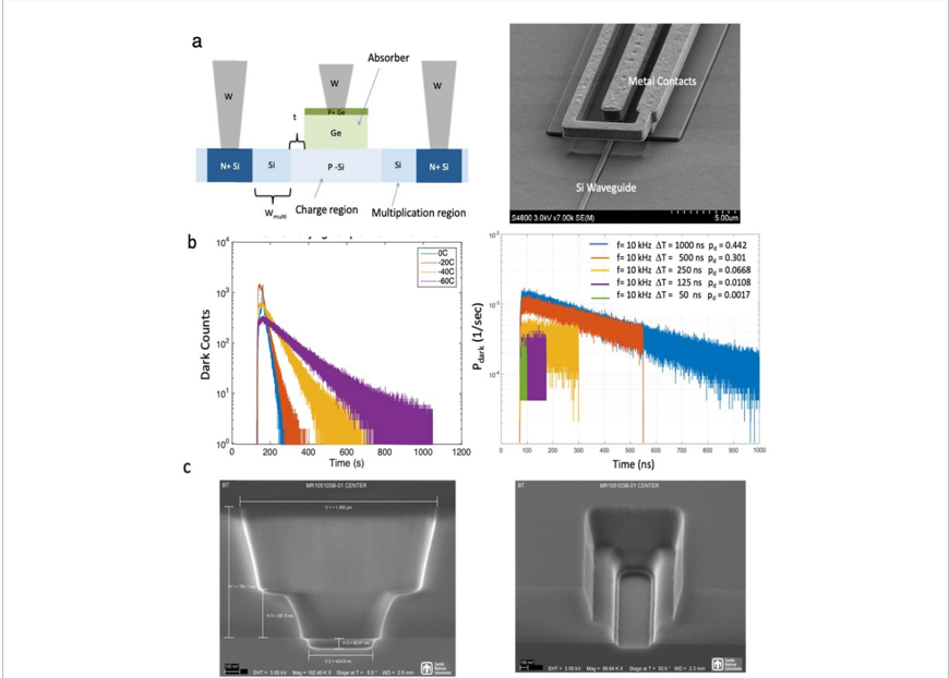
“Waveguide-integrated SNSPDs are central to quantum photonics as they enable scalable measurements of quantum states and their interference directly on-chip.”
§ ROADMAP 2022 Roadmap on integrated quantum photonics > Concluding remarks
A result the paper reports from its own data — it cites no other source for it, so there is none to check. The quote shows it is in the paper.
In the paper
“In the last decade, remarkable advances in quantum photonic integration have enabled table-top experiments to be scaled down to prototype chips with improvements in efficiency, robustness, and key performance metrics.”
§ ROADMAP 2022 Roadmap on integrated quantum photonics > Abstract
A result the paper reports from its own data — it cites no other source for it, so there is none to check. The quote shows it is in the paper.
In the paper
“They offer clear advantages with respect to control of nonlinear processes, size, weight, and power consumption, integration with pump lasers and other photonic components, and scalability of the underlying manufacturing processes.”
§ ROADMAP 2022 Roadmap on integrated quantum photonics > Concluding remarks
7 more claims
Create a free account to see all 12 claims and every source verdict.
Citations
Cites
Items 201–288 of 288
Emerging heterogeneous integrated photonic platforms on silicon
Fathpour, S. (2014) · Nanophotonics · doi:10.1515/nanoph-2014-0024 · Cited by 74 · cited 1×
“Future advances in quantum photonics will likely require a heterogeneous approach [14] that combines multiple PIC materials to achieve high-level functionality with integrated lasers and amplifiers, passive components, modulators, quantum frequency converters, efficient detectors or chip-to-fiber couplers, and control…”
BackgroundPrecise and diffraction-limited waveguide-to-free-space focusing gratings
Mehta, K. K., & Ram, R. J. (2017) · Scientific Reports · doi:10.1038/s41598-017-02169-2 · Cited by 69
Self-citationCryogenic operation of silicon photonic modulators based on the DC Kerr effect
Chakraborty, U., Carolan, J., Clark, G., Bunandar, D., Gilbert, G., Notaros, J., Watts, M. R., & Englund, D. R. (2020) · Optica · doi:10.1364/optica.403178 · Cited by 68 · cited 1×
“While silicon lacks a natural second-order nonlinearity, it is possible to induce one by applying DC fields that enables fast, cryogenically compatible switching [30].”
BackgroundExperimental quantum homodyne tomography via machine learning
Tiunov, E. S., Tiunova (Vyborova), V. V., Ulanov, A. E., Lvovsky, A. I., & Fedorov, A. K. (2020) · Optica · doi:10.1364/optica.389482 · Cited by 68
Quantum dot single-photon emission coupled into single-mode fibers with 3D printed micro-objectives
Bremer, L., Weber, K., Fischbach, S., Thiele, S., Schmidt, M., Kaganskiy, A., Rodt, S., Herkommer, A., Sartison, M., Portalupi, S. L., et al. (2020) · APL Photonics · doi:10.1063/5.0014921 · Cited by 68 · cited 1×
“Published results rely either on optical alignment in combination with gluing the fiber [142] or on micromechanical fiber holders and micro-optics [143, 144].”
MethodSelf-citationCastelletto, S. A., & Scholten, R. E. (2008) · The European Physical Journal Applied Physics · doi:10.1051/epjap:2008029 · Cited by 68
Controlling the spectrum of photons generated on a silicon nanophotonic chip
Kumar, R., Ong, J. R., Savanier, M., & Mookherjea, S. (2014) · Nature Communications · doi:10.1038/ncomms6489 · Cited by 65
Self-citationMid-infrared quantum optics in silicon
Rosenfeld, L. M., Sulway, D. A., Sinclair, G. F., Anant, V., Thompson, M. G., Rarity, J. G., & Silverstone, J. W. (2020) · Optics Express · doi:10.1364/oe.386615 · Cited by 64 · cited 1×
“Alternatively, recent work has demonstrated the advantages of operating at longer wavelengths within silicon, to heavily suppress TPA, thus reducing nonlinear propagation losses whilst retaining the full toolbox of silicon photonic components [27].”
BackgroundIon traps fabricated in a CMOS foundry
Mehta, K. K., Eltony, A. M., Bruzewicz, C. D., Chuang, I. L., Ram, R. J., Sage, J. M., & Chiaverini, J. (2014) · Applied Physics Letters · doi:10.1063/1.4892061 · Cited by 64
Self-citationGeneration of Non‐Classical Light Using Semiconductor Quantum Dots
Trivedi, R., Fischer, K. A., Vučković, J., & Müller, K. (2020) · Advanced Quantum Technologies · doi:10.1002/qute.201900007 · Cited by 64
Integration of diamond-based quantum emitters with nanophotonic circuits
Schrinner, P. P. J., Olthaus, J., Reiter, D. E., & Schuck, C. (2020) · Nano Letters · doi:10.1021/acs.nanolett.0c03262 · Cited by 63
Musiał, A., Holewa, P., Wyborski, P., Syperek, M., Kors, A., Reithmaier, J. P., Sek, G., & Benyoucef, M. (2019) · Advanced Quantum Technologies · doi:10.1002/qute.201900082 · Cited by 62
Integrated optical addressing of a trapped ytterbium ion
Ivory, M., Setzer, W. J., Karl, N., McGuinness, H., DeRose, C., Blain, M., Stick, D., Gehl, M., & Parazzoli, L. P. (2021) · Physical Review X · doi:10.1103/physrevx.11.041033 · Cited by 62
Self-citationPhoton-number-resolving superconducting nanowire detectors
Mattioli, F., Zhou, Z., Gaggero, A., Gaudio, R., Jahanmirinejad, S., Sahin, D., Marsili, F., Leoni, R., & Fiore, A. (2015) · Superconductor Science and Technology · doi:10.1088/0953-2048/28/10/104001 · Cited by 61
Savanier, M., Kumar, R., & Mookherjea, S. (2015) · Applied Physics Letters · doi:10.1063/1.4932047 · Cited by 60
Self-citationHughes, S., & Agarwal, G. S. (2017) · Physical Review Letters · doi:10.1103/physrevlett.118.063601 · Cited by 60 · cited 1×
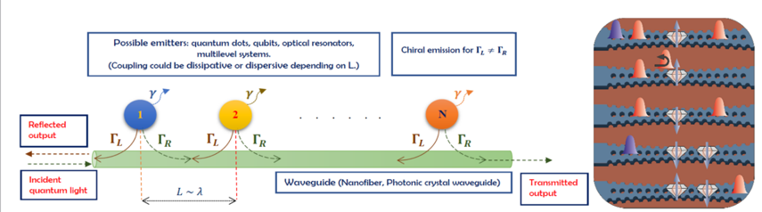
“All these ideas can be contextualized in a variety of experimental models of topical interest such as resonators on a transmission line, cold atoms near a fiber and QDs coupled to plasmonic excitations in a nanowire or photonic crystal waveguides [163, 164].”
BackgroundSelf-citationChartrand, C., Bergeron, L., Morse, K. J., Riemann, H., Abrosimov, N. V., Becker, P., Pohl, H.-J., Simmons, S., & Thewalt, M. L. W. (2018) · Physical Review B · doi:10.1103/physrevb.98.195201 · Cited by 60 · cited 5×
“The leading candidates are silicon-nitride (SiN), tantalum pentoxide (Ta2O5), alumina oxide (Al2O3), aluminium nitride (AlN), lithium niobate (LiNbO3) or similar high-bandgap materials providing good optical performance [7].”
BackgroundMethodInfluentialPlug&Play Fiber‐Coupled 73 kHz Single‐Photon Source Operating in the Telecom O‐Band
Musiał, A., Żołnacz, K., Srocka, N., Kravets, O., Große, J., Olszewski, J., Poturaj, K., Wójcik, G., Mergo, P., Dybka, K., et al. (2020) · Advanced Quantum Technologies · doi:10.1002/qute.202000018 · Cited by 56
Self-citationExact dissipation model for arbitrary photonic Fock state transport in waveguide QED systems
Chen, Z., Zhou, Y., & Shen, J.-T. (2017) · Optics Letters · doi:10.1364/ol.42.000887 · Cited by 53 · cited 1×
“Nevertheless, the impact of decoherence channels in generic waveguide-QED models has been theoretically studied from rigorous, first-principle considerations [167].”
BackgroundIntegrated photonic devices in single crystal diamond
Mi, S., Kiss, M., Graziosi, T., & Quack, N. (2020) · Journal of Physics: Photonics · doi:10.1088/2515-7647/aba171 · Cited by 53 · cited 33×
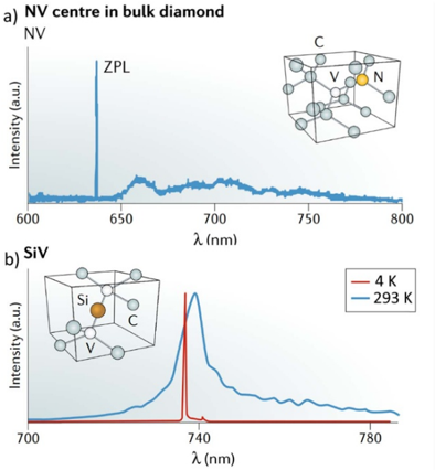
“Niels Quack (EPFL), Christophe Galland (EPFL), Igor Aharonovich (UTS) Status The unique combination of extraordinary physical and optical properties of high-purity single crystal diamond has propelled this material far beyond its traditional use as gemstone in jewellery, fostering a growing body of scientific research…”
BackgroundInfluentialZargaleh, S. A., Hameau, S., Eble, B., Margaillan, F., von Bardeleben, H. J., Cantin, J. L., & Gao, W. (2018) · Physical Review B · doi:10.1103/physrevb.98.165203 · Cited by 53
Optical waveguiding by atomic entanglement in multilevel atom arrays
Asenjo-Garcia, A., Kimble, H. J., & Chang, D. E. (2019) · Proceedings of the National Academy of Sciences · doi:10.1073/pnas.1911467116 · Cited by 53 · cited 1×
“Interestingly, the cold-atom community is now investigating not only multi-atomic systems coupled to waveguides, but also into possibilities of constructing waveguides from atomic arrays themselves [168].”
BackgroundSilicon as an emissive optical medium
Shainline, J. M., & Xu, J. (2007) · Laser & Photonics Reviews · doi:10.1002/lpor.200710021 · Cited by 52 · cited 8×
“1 b), which benefit from dispersion engineering in thick Ta2O5 layers that form without cracks due to the low intrinsic material stress [2].”
BackgroundInfluentialHeterogeneous silicon nitride photonics
Park, H., Zhang, C., Tran, M. A., & Komljenovic, T. (2020) · Optica · doi:10.1364/optica.391809 · Cited by 52
Scalable fabrication of optical resonators with embedded site-controlled quantum dots
Sünner, T., Schneider, C., Strauß, M., Huggenberger, A., Wiener, D., Höfling, S., Kamp, M., & Forchel, A. (2008) · Optics Letters · doi:10.1364/ol.33.001759 · Cited by 48
Low-loss low thermo-optic coefficient Ta2O5 on crystal quartz planar optical waveguides
Zhao, Q., Behunin, R. O., Rakich, P. T., Chauhan, N., Isichenko, A., Wang, J., Hoyt, C., Fertig, C., Lin, M. H., & Blumenthal, D. J. (2020) · APL Photonics · doi:10.1063/5.0024743 · Cited by 48 · cited 1×
“Especially interesting in this regard are the record low thermo-optic coefficient [66], enabling stable operation of high quality-factor devices, in particular at cryogenic temperatures, and the extremely low intrinsic photoluminescence, which is an indispensable requirement when working at the single-photon level.”
BackgroundSelf-citationRoom-temperature photonic logical qubits via second-order nonlinearities
Krastanov, S., Heuck, M., Shapiro, J. H., Narang, P., Englund, D. R., & Jacobs, K. (2021) · Nature Communications · doi:10.1038/s41467-020-20417-4 · Cited by 44 · cited 2×
“Since scalability of on-demand entangled-photon sources has not yet been realized, current practice relies on multiplexing probabilistic pair sources through linear optical gates and post-selection [6, 34], but other schemes have been proposed [96].”
BackgroundTantalum pentoxide nanophotonic circuits for integrated quantum technology
Splitthoff, L., Wolff, M. A., Grottke, T., & Schuck, C. (2020) · Optics Express · doi:10.1364/oe.388080 · Cited by 44 · cited 2×
“Importantly for realizing reconfigurable quantum photonic information processing systems, active and passive nanophotonic circuit components have been demonstrated with single-mode Ta2O5 waveguides [71].”
BackgroundSuperconducting nanowire single-photon detectors fabricated from atomic-layer-deposited NbN
Cheng, R., Wang, S., & Tang, H. X. (2019) · Applied Physics Letters · doi:10.1063/1.5131664 · Cited by 43
Self-citationMultiple Fano interferences due to waveguide-mediated phase coupling between atoms
Mukhopadhyay, D., & Agarwal, G. S. (2019) · Physical Review A · doi:10.1103/physreva.100.013812 · Cited by 43
Self-citationGrant, P. C., Dou, W., Alharthi, B., Grant, J. M., Tran, H., Abernathy, G., Mosleh, A., Du, W., Li, B., Mortazavi, M., et al. (2019) · Optical Materials Express · doi:10.1364/ome.9.003277 · Cited by 41 · cited 1×
“Recently, advances in selective epitaxial growth of strained Ge1−xSnx alloys have led to a new high-refractive-index semiconductor alloy with a tuneable direct bandgap for varying Sn concentration (x = 5%–20%) [216].”
BackgroundBakir, B. B., Seassal, C., Letartre, X., Regreny, P., Gendry, M., Viktorovitch, P., Zussy, M., Cioccio, L. D., & Fedeli, J. M. (2006) · Optics Express · doi:10.1364/oe.14.009269 · Cited by 40 · cited 2×
“Heterogeneous integration at the chip scale was used by Bakir et al [38] to produce, for the first time, optically pumped lasers based on III–V epitaxial QDs on a silicon substrate.”
MethodSrocka, N., Mrowiński, P., Große, J., von Helversen, M., Heindel, T., Rodt, S., & Reitzenstein, S. (2020) · Applied Physics Letters · doi:10.1063/5.0010436 · Cited by 40
Uniformity study of wafer-scale InP-to-silicon hybrid integration
Liang, D., Chapman, D. C., Li, Y., Oakley, D. C., Napoleone, T., Juodawlkis, P. W., Brubaker, C., Mann, C., Bar, H., Raday, O., et al. (2011) · Applied Physics A · doi:10.1007/s00339-010-5999-z · Cited by 39 · cited 1×
“While much of the initial work involved bonding at the chip scale, bonding at the wafer scale was later also demonstrated [37].”
BackgroundSelf-citationNanophotonic tantala waveguides for supercontinuum generation pumped at 1560 nm
Lamee, K. F., Carlson, D. R., Newman, Z. L., Yu, S.-P., & Papp, S. B. (2020) · Optics Letters · doi:10.1364/ol.396950 · Cited by 39
Millimeter-wave interconnects for microwave-frequency quantum machines
Pechal, M., & Safavi-Naeini, A. H. (2017) · Physical Review A · doi:10.1103/physreva.96.042305 · Cited by 38 · cited 20×
“For resonator-based modulators, this bandwidth is restricted to tens of GHz by the width of the optical resonance and resistance-capacitance limit of the electrode.”
BackgroundInfluentialSelf-citationSingle-photon superradiant emission rate scaling for atoms trapped in a photonic waveguide
Zhou, Y., Chen, Z., & Shen, J.-T. (2017) · Physical Review A · doi:10.1103/physreva.95.043832 · Cited by 38 · cited 1×
“scaling decay rate, as has been demonstrated in [159, 161].”
ResultHeterogeneous Integration Roadmap: Driving Force and Enabling Technology for Systems of the Future
Chen, W. C., & Bottoms, B. (2019) · Symposium on VLSI Technology · doi:10.23919/vlsit.2019.8776484 · Cited by 37 · cited 1×
“Advancing towards heterogeneous integration [262] is therefore a crucial challenge, and will also be of great importance for ultimately integrating also the electronic functionalities of the system needed for signal control and data processing.”
BackgroundHigh-Power (>300 mW) On-Chip Laser With Passively Aligned Silicon-Nitride Waveguide DBR Cavity
Kharas, D., Plant, J. J., Loh, W., Swint, R. B., Bramhavar, S., Heidelberger, C., Yegnanarayanan, S., & Juodawlkis, P. W. (2020) · IEEE Photonics Journal · doi:10.1109/jphot.2020.3037834 · Cited by 34 · cited 2×
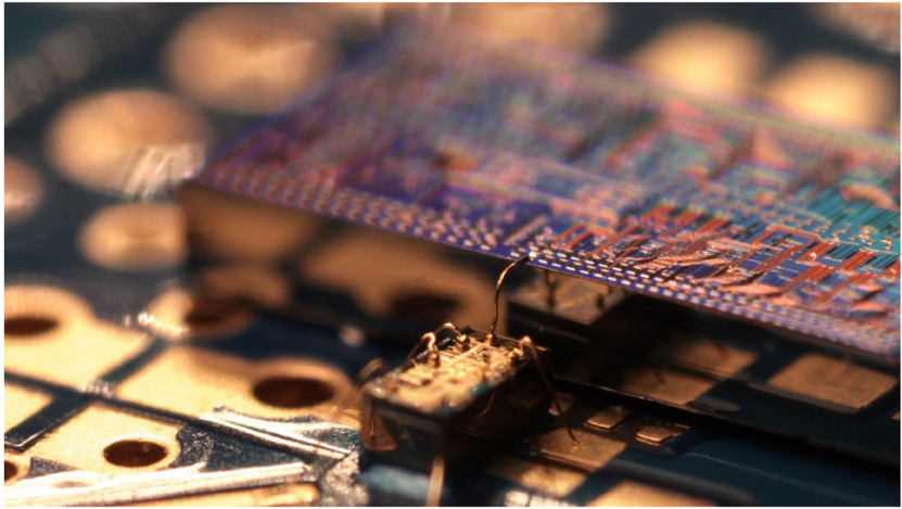
“Panel (d) reprinted with permission from [17] under a Creative Commons License.”
BackgroundMethodSelf-citationSuperconducting nanowire single-photon detectors integrated with tantalum pentoxide waveguides
Wolff, M. A., Vogel, S., Splitthoff, L., & Schuck, C. (2020) · Scientific Reports · doi:10.1038/s41598-020-74426-w · Cited by 33
Self-citationErbium-doped waveguide laser in tantalum pentoxide
Subramani, A. Z., Oton, C. J., Shepherd, D. P., & Wilkinson, J. S. (2010) · IEEE Photonics Technology Letters · doi:10.1109/lpt.2010.2072495 · Cited by 32 · cited 1×
“Moreover, Ta2O5 can host rare-earth ions, including erbium [67], which enables use as a gain medium, thus providing optical signal amplification and lasing capabilities on-chip.”
BackgroundHigh-Q-factor nanobeam photonic crystal cavities in bulk silicon carbide
Song, B.-S., Jeon, S., Kim, H., Kang, D. D., Asano, T., & Noda, S. (2018) · Applied Physics Letters · doi:10.1063/1.5058194 · Cited by 31 · cited 1×
“Nevertheless, several successful directions have been pursued: photo-electrochemical etching [124], SiC thinning and bonding onto an insulator [125], and Faraday-cage angled etching [131].”
BackgroundTransparency in a chain of disparate quantum emitters strongly coupled to a waveguide
Mukhopadhyay, D., & Agarwal, G. S. (2020) · Physical Review A · doi:10.1103/physreva.101.063814 · Cited by 31 · cited 2×
“Possibility of transparency due to single-photon transport across differentially detuned two-level emitters has been theoretically demonstrated, without applying any control field [160].”
BackgroundControlled integration of selected detectors and emitters in photonic integrated circuits
Gourgues, R., Zadeh, I. E., Elshaari, A. W., Bulgarini, G., Los, J. W. N., Zichi, J., Dalacu, D., Poole, P. J., Dorenbos, S. N., & Zwiller, V. (2019) · Optics Express · doi:10.1364/oe.27.003710 · Cited by 30 · cited 1×
“via pick-and-place approaches [204] or by photonic circuit fabrication on top of pre-selected nanowire devices [205].”
MethodSelf-citationA tuneable telecom wavelength entangled light emitting diode deployed in an installed fibre network
Xiang, Z.-H., Huwer, J., Skiba-Szymanska, J., Stevenson, R. M., Ellis, D. J. P., Farrer, I., Ward, M. B., Ritchie, D. A., & Shields, A. J. (2020) · Communications Physics · doi:10.1038/s42005-020-0390-7 · Cited by 29
Single photon detection with superconducting nanowires on crystalline silicon carbide
Martini, F., Gaggero, A., Mattioli, F., & Leoni, R. (2019) · Optics Express · doi:10.1364/oe.27.029669 · Cited by 23 · cited 1×
“Recently, the first SNSPDs on 3C-SiC substrate were implemented [134].”
BackgroundContinuous and time-domain coherent signal conversion between optical and microwave frequencies
Peairs, G. A., Chou, M.-H., Bienfait, A., Chang, H.-S., Conner, C. R., Dumur, É., Grebel, J., Povey, R. G., Şahin, E., Satzinger, K. J., et al. (2020) · Physical Review Applied · doi:10.1103/physrevapplied.14.061001 · Cited by 21
Microring resonator-coupled photoluminescence from silicon W centers
Tait, A. N., Buckley, S. M., Chiles, J., McCaughan, A. N., Olson, S., Rao, S. P., Nam, S. W., Mirin, R. P., & Shainline, J. M. (2020) · Journal of Physics: Photonics · doi:10.1088/2515-7647/ab95f2 · Cited by 21
Self-citationQin, J., Shu, H., Chang, L., Xie, W., Tao, Y., Jin, M., Wang, X., & Bowers, J. E. (2020) · Optics Letters · doi:10.1364/ol.398777 · Cited by 21 · cited 2×
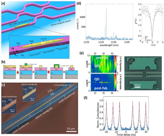
“Panel (f) reprinted with permission from [49].”
MethodSelf-citationMcDonald, C., Moody, G., Nam, S. W., Mirin, R. P., Shainline, J. M., McCaughan, A., Buckley, S., & Silverman, K. L. (2019) · Applied Physics Letters · doi:10.1063/1.5108893 · Cited by 20 · cited 1×
“Importantly, those modulators are suitable to work under cryogenic temperature, which are required for operating QD-based single photon emitters as well as superconducting nanowire single-photon detectors (SNSPDs), which recently has also been successfully integrated on GaAs waveguides [51].”
BackgroundParasitic photon-pair suppression via photonic stop-band engineering
Helt, L. G., Brańczyk, A. M., Liscidini, M., & Steel, M. J. (2017) · Physical Review Letters · doi:10.1103/physrevlett.118.073603 · Cited by 19 · cited 1×
“A dual-pump SFWM process can be used to generate frequency-degenerate signal and idler photons, with some additional considerations for noise management [102].”
MethodSrocka, N., Mrowiński, P., Große, J., Schmidt, M., Rodt, S., & Reitzenstein, S. (2020) · Applied Physics Letters · doi:10.1063/5.0030991 · Cited by 19
Self-citationRealities and challenges of III-V/Si integration technologies
Bowers, J. E., Huang, D., Jung, D., Norman, J., Tran, M. A., Wan, Y., Xie, W., & Zhang, Z. (2019) · Optical Fiber Communication Conference (OFC) 2019 · doi:10.1364/ofc.2019.tu3e.1 · Cited by 19 · cited 1×
“The approach has been applied in the fabrication of optoelectronic [35] and nonlinear photonic [36] devices on silicon substrates and on-chip waveguides, with gain, absorption and enhanced optical nonlinearities provided by III–V semiconductor materials.”
MethodSelf-citationEfficient bidirectional piezo-optomechanical transduction between microwave and optical frequency
Jiang, W., Sarabalis, C. J., Dahmani, Y. D., Patel, R. N., Mayor, F. M., McKenna, T. P., Laer, R. V., & Safavi‐Naeini, A. H. (2020) · Conference on Lasers and Electro-Optics · doi:10.1364/cleo_at.2020.af3k.4 · Cited by 17
Self-citationScalable Quantum Photonics with Single Color Centers in Silicon Carbide
Radulaski, M., Widmann, M., Niethammer, M., Zhang, J. L., Lee, S.-Y., Rendler, T., Lagoudakis, K. G., Son, N. T., Janzen, E., Ohshima, T., et al. (2017) · Conference on Lasers and Electro-Optics · doi:10.1364/cleo_at.2017.jm3e.4 · Cited by 15
Self-citationPetrov, N. L., Fedotov, A. B., & Zheltikov, A. M. (2019) · Optics Communications · doi:10.1016/j.optcom.2019.04.084 · Cited by 14
Self-citation(2017) · DSpace@MIT (Massachusetts Institute of Technology) · Cited by 14
Ultra-high Q Resonators and Sub-GHz Bandwidth Second Order Filters in an SOI Foundry Platform
Onural, D., Gevorgyan, H., Zhang, B., Khilo, A. N., & Popović, M. A. (2020) · Optical Fiber Communication Conference · doi:10.1364/ofc.2020.w1a.4 · Cited by 11
Low-loss thin-film lithium niobate bonded on silicon nitride waveguides
Ghosh, S., Yegnanarayanan, S., Ricci, M., Kharas, D., & Juodawlkis, P. (2020) · Conference on Lasers and Electro-Optics · doi:10.1364/cleo_si.2020.sth1f.1 · Cited by 11 · cited 2×
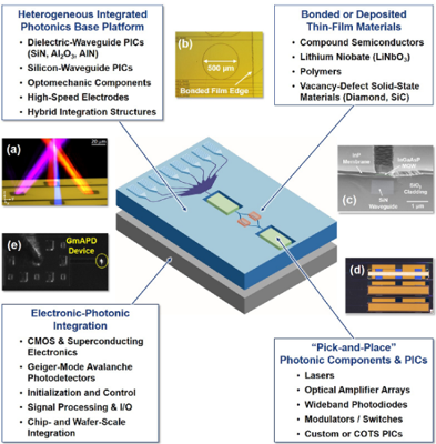
“Exemplar demonstrations of such a heterogeneous PIC platform include high-power (>300 mW) low-noise lasers incorporating flip-chipped semiconductor optical amplifiers (figure 3(d)) [17], surface-bonded optical gain media (figure 3(c)) [18, 19], and low-loss surface-bonded thin-film lithium-niobate (TFLN) waveguides (f…”
BackgroundSelf-citationLu, X., Moille, G., Rao, A., & Srinivasan, K. (2021) · Optics Letters · doi:10.1364/ol.412602 · Cited by 11 · cited 1×
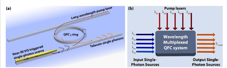
“For example, four-wave mixing QFC between 980 and 1550 nm (on-chip efficiency≈60%) was recently shown in SiN microrings [183] and constituted a wider spectral gap than previous demonstrations in optical fibers; efficient and low-noise visible-to-telecom QFC has also been proposed using similar devices [184].”
MethodSelf-citationSOH Mach-Zehnder Modulators for 100 GBd PAM4 Signaling With Sub-1 dB Phase-Shifter Loss
Kieninger, C., Füllner, C., Zwickel, H., Kutuvantavida, Y., Kemal, J. N., Eschenbaum, C., Elder, D. L., Dalton, L. R., Freude, W., Randel, S., et al. (2020) · Optical Fiber Communication Conference · doi:10.1364/ofc.2020.th3c.3 · Cited by 11
Cavity-enhanced second harmonic generation via nonlinear-overlap optimization
Lin, Z., Liang, X., Lončar, M., Johnson, S. G., & Rodríguez, A. W. (2015) · Frontiers in Optics · doi:10.1364/fio.2015.fm1d.3 · Cited by 10
Self-citationSavanier, M., & Mookherjea, S. (2016) · Applied Physics Letters · doi:10.1063/1.4954261 · Cited by 9
Self-citationAn Integrated Diamond Nanophotonics Platform for Quantum Optical Networks
Sipahigil, A. (2017) · Conference on Lasers and Electro-Optics · doi:10.1364/cleo_qels.2017.fth3h.4 · Cited by 8
Petrov, N. L., Voronin, A. A., Fedotov, A. B., & Zheltikov, A. M. (2019) · Applied Physics B · doi:10.1007/s00340-019-7138-7 · Cited by 6
Self-citationHeterogeneous silicon nitride photonics: erratum
Park, H., Zhang, C., Tran, M. A., & Komljenović, T. (2020) · Optica · doi:10.1364/optica.395210 · Cited by 5
Riedel, D., Söllner, I., Shields, B., Starosielec, S., Appel, P., Neu, E., Maletinsky, P., & Warburton, R. J. (2017) · Quantum Photonic Devices · doi:10.1117/12.2277514 · Cited by 4
Rapid Simulation of Scattering Parameters for Coupled Waveguides With Arbitrary Geometries
Potokar, E. R., Collings, R. S., Hammond, A. M., et al. (2020) · Journal of Lightwave Technology · doi:10.1109/jlt.2020.3028807 · Cited by 3 · cited 1×
“There continues to be rapid advances in forward solutions in the form of compact models and abstractions, many of which incorporate machine learning as subroutines [273].”
BackgroundSelf-citationInGaAsP/InP membrane gain sections for III-V/SiNx heterogeneous photonic integration
Heidelberger, C., Santis, C. T., Plant, J. J., Morissette, E. M., Kharas, D., Swint, R. B., Yariv, A., & Juodawlkis, P. W. (2021) · Conference on Lasers and Electro-Optics · doi:10.1364/cleo_si.2021.sth2h.1 · Cited by 3 · cited 1×
“Exemplar demonstrations of such a heterogeneous PIC platform include high-power (>300 mW) low-noise lasers incorporating flip-chipped semiconductor optical amplifiers (figure 3(d)) [17], surface-bonded optical gain media (figure 3(c)) [18, 19], and low-loss surface-bonded thin-film lithium-niobate (TFLN) waveguides (f…”
BackgroundSelf-citationWaveguide engineering for hybrid Si/III-V lasers and amplifiers
Swint, R. B., Spector, S. J., Chen, C. L., Plant, J. J., Lyszczarz, T., & Juodawlkis, P. W. (2012) · Conference on Lasers and Electro-Optics 2012 · doi:10.1364/cleo_si.2012.ctu2n.7 · Cited by 3 · cited 1×
“Exemplar demonstrations of such a heterogeneous PIC platform include high-power (>300 mW) low-noise lasers incorporating flip-chipped semiconductor optical amplifiers (figure 3(d)) [17], surface-bonded optical gain media (figure 3(c)) [18, 19], and low-loss surface-bonded thin-film lithium-niobate (TFLN) waveguides (f…”
BackgroundSelf-citationLasers on silicon by heteroepitaxy
Klamkin, J., Shi, B., Wang, L., Brunelli, S. S., Song, B., & Meissner, T. (2020) · 2020 IEEE Photonics Conference (IPC) · doi:10.1109/ipc47351.2020.9252454 · Cited by 2
Harnessing spectral phase in broadband time-energy entangled photons for precision delay sensing
Seshadri, S., Imany, P., Lingaraju, N., Leaird, D. E., & Weiner, A. M. (2020) · Frontiers in Optics / Laser Science · doi:10.1364/fio.2020.fw7c.1 · Cited by 2
Self-citationPuckett, M. W., Liu, K., Chauhan, N., et al. (2020) · Research Square · doi:10.21203/rs.3.rs-65823/v1 · Cited by 2
Lithium-niobate-on-insulator waveguide-integrated superconducting nanowire single-photon detectors
Sayem, A. A., Cheng, R., Wang, S., & Tang, H. X. (2020) · Applied Physics Letters · doi:10.1063/1.5142852 · Cited by 1
Ultrahigh-Q Lithium Niobate Microring Resonator
Zhang, M., Wang, C., Cheng, R., Shams‐Ansari, A., & Lončar, M. (2018) · Conference on Lasers and Electro-Optics · doi:10.1364/cleo_si.2018.sf2i.3 · Cited by 1
Self-citationEntangled Photon Pair Generation from an AlGaAs-on-Insulator Microring Resonator
Steiner, T. J., Castro, J. E., Chang, L., Dang, Q. T., Xie, W., Li, C., Norman, J., Bowers, J. E., & Moody, G. (2021) · Conference on Lasers and Electro-Optics · doi:10.1364/cleo_qels.2021.fth1o.4
Self-citationA Reconfigurable Photonic Chip for Generating, Manipulating and Measuring Entanglement and Mixture
Shadbolt, P., Verde, M. R., Peruzzo, A., Politi, A., Laing, A., Lobino, M., Matthews, J. C. F., Thompson, M. G., & O’Brien, J. L. (2012) · Conference on Lasers and Electro-Optics · doi:10.1364/qels.2012.qf2f.1
Self-citationCryogenic Operation of DC Kerr Silicon Photonic Modulators
Chakraborty, U., Carolan, J., Clark, G., Bunandar, D., Gilbert, G. N., Notaroš, J., Watts, M. R., & Englund, D. R. (2021) · Conference on Lasers and Electro-Optics · doi:10.1364/cleo_si.2021.sth1q.1
Quantum Dot Single-Photon Emission Coupled into Single-Mode Fibers with 3D Printed Micro-Objectives
Bremer, L., Weber, K., Fischbach, S., Thiele, S., Schmidt, M., Kaganskiy, A., Rodt, S., Herkommer, A., Sartison, M., Portalupi, S. L., et al. (2021) · Conference on Lasers and Electro-Optics · doi:10.1364/cleo_at.2021.atu2s.5
Self-citationZhao, J., Ma, C., Rüsing, M., & Mookherjea, S. (2019) · Frontiers in Optics · doi:10.1364/fio.2019.ftu6a.3
Self-citationXue, G.-T., Niu, Y.-F., Liu, X., et al. (2020) · arXiv · doi:10.48550/arxiv.2012.06092
Integrated optical addressing of a trapped ytterbium ion
Ivory, M., Setzer, W. J., Karl, N., et al. (2020) · arXiv · doi:10.48550/arxiv.2011.12376
Multifunctional on-chip storage at telecommunication wavelength for quantum networks
Craiciu, I., Lei, M., Rochman, J., et al. (2020) · arXiv · doi:10.48550/arxiv.2008.10795
Full daylight quantum-key-distribution at 1550 nm enabled by integrated silicon photonics
Avesani, M., Calderaro, L., Schiavon, M., et al. (2019) · arXiv · doi:10.48550/arxiv.1907.10039
Error protected qubits in a silicon photonic chip
Vigliar, C., Paesani, S., Ding, Y., et al. (2020) · arXiv · doi:10.48550/arxiv.2009.08339
Author Correction: Ultra-efficient frequency comb generation in AlGaAs-on-insulator microresonators
Chang, L., Xie, W., Shu, H., et al. (2021) · Nature Communications · doi:10.1038/s41467-021-22031-4
Self-citationArnold, G., Wulf, M., Barzanjeh, S., et al. (2020) · Nature Communications · doi:10.1038/s41467-020-18912-9
Driving Force and Enabling Technology for Systems of the Future
Chen, W. (2019) · International Symposium on Microelectronics · doi:10.4071/2380-4505-2019.1.invitedhir000001
Research works printed but not linked: 4
- 72. Maleki L and Matsko A 2009 Ferroelectric Crystals for Photonic Applications (Berlin: Springer)
- 188. Girvin M 2014 Circuit QED: superconducting qubits coupled to microwave photons Quantum Machines: Measurement and Control ofEngineered Quantum Systems (Les Houches Summer School, Session XCVI) ed M Devoret, B Huard, R Schoelkopf and L F Cugliandolo (Oxford: Oxford University ) pp 113-255
- 189. Juanjuan L, Ming L, Zou C-L, Al Sayem A and Tang H X 2020 Towards 1% single photon nonlinearity with periodically-poled lithium niobate microring resonators Optica 7 1654 · DOI · Paper page
- 231. Rungta P, Munro W J, Nemoto K, Deuar P, Milburn G J and Caves C M 2001 Qudit entanglement Directions in Quantum Optics: A Collection of Papers Dedicated to the Memory of Dan Walls ed H J Carmichael, R J Glauber and M O Scully (Berlin: Springer) pp 149-64
Cited by
Applications of optical microcombs
Sun, Y., Wu, J., Tan, M., Xu, X., Li, Y., Morandotti, R., Mitchell, A., & Moss, D. J. (2023) · Advances in Optics and Photonics · doi:10.1364/aop.470264 · Cited by 302
Corato-Zanarella, M., Gil-Molina, A., Ji, X., Shin, M. C., Mohanty, A., & Lipson, M. (2023) · Nature Photonics · doi:10.1038/s41566-022-01120-w · Cited by 233
Integrated Electro-Optics on Thin-Film Lithium Niobate
Hu, Y., Zhu, D., Lu, S., Zhu, X., Song, Y., Renaud, D., Assumpcao, D., Cheng, R., Xin, C. J., Yeh, M., et al. (2025) · Nature Reviews Physics · doi:10.1038/s42254-025-00825-5 · Cited by 162
“The properties of TFLN, including low-loss, possibility of large scale integration, possibility for photon-photon interactions through EO and/or optical 𝜒 (2) , render it an attractive platform for generating and manipulating quantum states of light 175 .”
Self-citationSingle-photon detection and cryogenic reconfigurability in lithium niobate nanophotonic circuits
Lomonte, E., Wolff, M. A., Beutel, F., Ferrari, S., Schuck, C., Pernice, W. H. P., & Lenzini, F. (2021) · Nature Communications · doi:10.1038/s41467-021-27205-8 · Cited by 163
Self-citationChip-based laser with 1-hertz integrated linewidth
Guo, J., McLemore, C. A., Xiang, C., Lee, D., Wu, L., Jin, W., Kelleher, M., Jin, N., Mason, D., Chang, L., et al. (2022) · Science Advances · doi:10.1126/sciadv.abp9006 · Cited by 112
Metadata
- Authors
- Moody, G., Sorger, V. J., Blumenthal, D. J., Juodawlkis, P. W., Loh, W., Sorace-Agaskar, C., Jones, A. E., Balram, K. C., Matthews, J. C. F., Laing, A., Davanco, M., Chang, L., Bowers, J. E., Quack, N., Galland, C., Aharonovich, I., Wolff, M. A., Schuck, C., Sinclair, N., Lončar, M., Komljenovic, T., Weld, D., Mookherjea, S., Buckley, S., Radulaski, M., Reitzenstein, S., Pingault, B., Machielse, B., Mukhopadhyay, D., Akimov, A., Zheltikov, A., Agarwal, G. S., Srinivasan, K., Lu, J., Tang, H. X., Jiang, W., McKenna, T. P., Safavi-Naeini, A. H., Steinhauer, S., Elshaari, A. W., Zwiller, V., Davids, P. S., Martinez, N., Gehl, M., Chiaverini, J., Mehta, K. K., Romero, J., Lingaraju, N. B., Weiner, A. M., Peace, D., Cernansky, R., Lobino, M., Diamanti, E., Vidarte, L. T., & Camacho, R. M.
- Affiliations
- University of California, Santa Barbara (US)
- George Washington University (US)
- MIT Lincoln Laboratory (US)
- University of Bristol (GB)
- École Polytechnique Fédérale de Lausanne (CH)
- University of Technology Sydney (AU)
- University of Münster (DE)
- Harvard University (US)
- University of California San Diego (US)
- National Institute of Standards and Technology (US)
- University of California, Davis (US)
- Technische Universität Berlin (DE)
- Texas A&M University (US)
- P.N. Lebedev Physical Institute of the Russian Academy of Sciences (RU)
- Yale University (US)
- Stanford University (US)
- KTH Royal Institute of Technology (SE)
- Sandia National Laboratories (US)
- ETH Zurich (CH)
- Australian Research Council (AU)
- Purdue University West Lafayette (US)
- Griffith University (AU)
- Centre National de la Recherche Scientifique (FR)
- Brigham Young University (US)
- Corresponding author
- Moody, Galan
- ORCID
- Moody, Galan
- Sorger, Volker J
- Blumenthal, Daniel J
- Juodawlkis, Paul W
- Loh, William
- Sorace-Agaskar, Cheryl
- Balram, Krishna C
- Matthews, Jonathan C F
- Chang, Lin
- Bowers, John E
- Quack, Niels
- Galland, Christophe
- Aharonovich, Igor
- Wolff, Martin A
- Schuck, Carsten
- Sinclair, Neil
- Lončar, Marko
- Weld, David
- Mookherjea, Shayan
- Buckley, Sonia
- Radulaski, Marina
- Reitzenstein, Stephan
- Pingault, Benjamin
- Machielse, Bartholomeus
- Mukhopadhyay, Debsuvra
- Akimov, Alexey
- Zheltikov, Aleksei
- Agarwal, Girish S
- Srinivasan, Kartik
- Lu, Juanjuan
- Tang, Hong X
- Jiang, Wentao
- McKenna, Timothy P
- Safavi-Naeini, Amir H
- Steinhauer, Stephan
- Elshaari, Ali W
- Zwiller, Val
- Davids, Paul S
- Martinez, Nicholas
- Gehl, Michael
- Chiaverini, John
- Mehta, Karan K
- Romero, Jacquiline
- Lingaraju, Navin B
- Weiner, Andrew M
- Peace, Daniel
- Lobino, Mirko
- Diamanti, Eleni
- Vidarte, Luis Trigo
- Camacho, Ryan M
- Venue
- Journal of Physics: Photonics
- Publisher
- IOP Publishing
- Published
- 2022-01-01
- Volume
- 4
- Issue
- 1
- Pages
- 012501
- ISSN
- 2515-7647 (ISSN-L)
- OpenAlex
- W3128101795
- Cited by
- 6
- References
- 274
- Citations by year
- 2024: 2 · 2022: 2
- FWCI
- 0.44
- Type
- journal article
- Language
- en
- Open access
- gold
- doi.org
- Licence
- cc-by
- creativecommons.org/licenses/by/4.0 (vor, 30 d)
- iopscience.iop.org/info/page/text-and-data-mining (tdm, 30 d)
- Locations
- Journal of Physics Photonics (publishedVersion, cc-by)
- Explore Bristol Research (publishedVersion, cc-by)
- arXiv (Cornell University) (submittedVersion)
- HAL (submittedVersion)
- DepositOnce (submittedVersion, cc-by)
- eScholarship (California Digital Library) (submittedVersion)
- Infoscience (Ecole Polytechnique Fédérale de Lausanne) (submittedVersion, cc-by-nc-nd)
- Bristol Research (University of Bristol) (submittedVersion, cc-by)
- Griffith Research Online (submittedVersion, cc-by)
- Research Repository (Delft University of Technology) (submittedVersion)
- Repository for Publications and Research Data (ETH Zurich) (submittedVersion, cc-by)
- Data Archiving and Networked Services (DANS) (submittedVersion, cc-by)
- arXiv (Cornell University) (cc-by)
- Technische Universität Berlin – Universitätsbibliothek (cc-by)
- ETH Zürich Research Collection
- Funders
- National Science Foundation (1640968, FA8702-15-D-0001, 1941583, 1820930)
- U.S. Department of Defense (FA8702-15-D-0001)
- U.S. Department of Energy (FA8702-15-D-0001)
- National Aeronautics and Space Administration (FA8702-15-D-0001)
- Texas A and M University
- Westpac Bicentennial Foundation
- Keysight Technologies
- European Commission
- Deutsche Forschungsgemeinschaft
- Schweizerischer Nationalfonds zur Förderung der Wissenschaftlichen Forschung
- Russian Foundation for Basic Research
- Vetenskapsrådet
- Russian Science Foundation
- Ministry of Science and Higher Education of the Russian Federation
- National Institute of Standards and Technology
- Defense Advanced Research Projects Agency (FA8702-15-D-0001)
- National Nuclear Security Administration
- University of California, Santa Barbara
- Advanced Research Projects Agency
- Natural Sciences and Engineering Research Council of Canada
- Engineering and Physical Sciences Research Council (EP/T001062/1, EP/N003470/1)
- European Regional Development Fund
- Office of Naval Research (FA8702-15-D-0001, -0001)
- Basic Energy Sciences
- Air Force Office of Scientific Research (FA8702-15-D-0001)
- Army Research Office (FA8702-15-D-0001)
- Sandia National Laboratories
- Air Force Research Laboratory (FA8702‐15‐D‐0001)
- H2020 Marie Skłodowska-Curie Actions
- Division of Materials Sciences and Engineering
- Topics
- Physical Sciences › Engineering › Electrical and Electronic Engineering › Photonic and Optical Devices
- Physical Sciences › Physics and Astronomy › Atomic and Molecular Physics, and Optics › Quantum Information and Cryptography
- Physical Sciences › Computer Science › Artificial Intelligence › Quantum Computing Algorithms and Architecture
- Keywords
- integrated quantum photonics, quantum photonic integrated circuits, photonic platform, quantum light sources, quantum frequency conversion, quantum computing, quantum communication, quantum sensing
About these checks
Registry, retraction, Cites and statistics results are computed, not judged, with one exception: a printed reference that no index lists is read once by a model before it counts as a citation error. Claims are extracted by a model and kept only when their quote appears verbatim in the text; each cited source is then checked, with a model’s help, for whether it says what the claim relies on. Those verdicts can be wrong — read the claim’s quote and the cited source before relying on one.
A language model drew the claims from the paper on 2026-09-26 (prompt extract-v2).
Cited sources are checked with a language model’s help (gpt-6-sol).
Statistics and arithmetic are recomputed, not judged.
Confidence bands are shown only for fields calibrated on our annotated test set. None is calibrated yet, so no band is shown.
What counts as a claim ›How we measure confidence ›How we check this ›
Are you an author, or do you see a problem with this page? Request a review
Data sources
Bibliographic data: Semantic Scholar, OpenAlex, Crossref.
Contains information from the Semantic Scholar Academic Graph Datasets, made available under the ODC Attribution License (ODC-BY 1.0).
Semantic Scholar’s data is described in: Kinney, R., et al. (2023). The Semantic Scholar Open Data Platform. arXiv:2301.10140.
